NTC Proprietary
Level: Property
DDR3(L)-2Gb SDRAM
NT5CB(C)256M8JQ/NT5CB(C)128M16JR
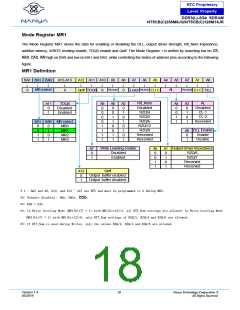
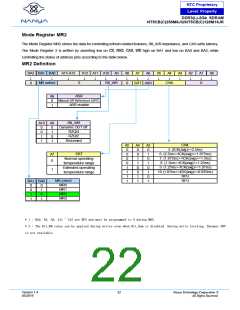
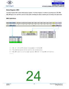
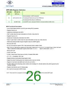
Mode Register MR2
The Mode Register MR2 stores the data for controlling refresh related features, Rtt_WR impedance, and CAS write latency.
The Mode Register 2 is written by asserting low on , RA, A, WE high on BA1 and low on BA0 and BA2, while
controlling the states of address pins according to the table below.
MR2 Definition
BA2 BA1 BA0
A15-A13
A12 A11 A10 A9
A8
↓
0
A7
A6
A5
A4
A3
A2
A1
A0
↓
↓
↓
↓
↓
↓
↓
↓
↓
↓
↓
↓
CWL
↓
↓
↓
0
↓
MR select
0
Rtt_WR
0
SRT ASR
ASR
A6
0
1
Manual SR Reference (SRT)
ASR enable
Rtt_WR
Dynamic ODT off
RZQ/4
A10 A9
0
0
1
1
0
1
0
1
RZQ/2
Reserved
CWL
5 (tCK(avg)>=2.5ns)
A5
0
A4
0
A3
0
SRT
6 (2.5ns>=tCK(avg)>=1.875ns)
7 (1.875ns>=tCK(avg)>=1.5ns)
8 (1.5ns>=tCK(avg)>=1.25ns)
9 (1.25ns>=tCK(avg)>=1.07ns)
10 (1.07ns>=tCK(avg)>=0.935ns)
RFU
A7
0
0
0
0
1
1
1
0
1
1
0
0
1
1
0
1
0
1
0
Normal operating
temperature range
Extended operating
temperature range
1
MR select
MR0
RFU
BA1 BA0
1
1
1
0
0
1
1
0
1
0
1
MR1
MR2
MR3
* 1 : BA2, A5, A8, A11 ~ A15 are RFU and must be programmed to 0 during MRS.
* 2 : The Rtt_WR value can be applied during writes even when Rtt_Nom is disabled. During write leveling, Dynamic ODT
is not available.
Version 1.4
05/2019
22
Nanya Technology Cooperation ©
All Rights Reserved.

 NANYA [ Nanya Technology Corporation. ]