NTC Proprietary
Level: Property
DDR3(L)-2Gb SDRAM
NT5CB(C)256M8JQ/NT5CB(C)128M16JR
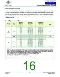
Burst Length, Type, and Order
Accesses within a given burst may be programmed to sequential or interleaved order. The burst type is selected via bit A3
as shown in the MR0 Definition as above figure. The ordering of access within a burst is determined by the burst length,
burst type, and the starting column address. The burst length is defined by bits A0-A1. Burst lengths options include fix
BC4, fixed BL8, and on the fly which allow BC4 or BL8 to be selected coincident with the registration of a Read or Write
command via A12/.
Burst Type and Burst Order
Starting
Column
Address
(A2,A1,A0)
Burst type:
Sequential
(decimal)
A3 = 0
Burst type:
Interleaved
(decimal)
A3 = 1
Burst
Length
Read
Write
Note
0,0,0
0,0,1
0,1,0
0,1,1
1,0,0
1,0,1
1,1,0
1,1,1
0,V,V
1,V,V
0,0,0
0,0,1
0,1,0
0,1,1
1,0,0
1,0,1
1,1,0
1,1,1
V,V,V
0,1,2,3,T,T,T,T
1,2,3,0,T,T,T,T
2,3,0,1,T,T,T,T
3,0,1,2,T,T,T,T
4,5,6,7,T,T,T,T
5,6,7,4,T,T,T,T
6,7,4,5,T,T,T,T
7,4,5,6,T,T,T,T
0,1,2,3,X,X,X,X
4,5,6,7,X,X,X,X
0,1,2,3,4,5,6,7
1,2,3,0,5,6,7,4
2,3,0,1,6,7,4,5
3,0,1,2,7,4,5,6
4,5,6,7,0,1,2,3
5,6,7,4,1,2,3,0
6,7,4,5,2,3,0,1
7,4,5,6,3,0,1,2
0,1,2,3,4,5,6,7
0,1,2,3,T,T,T,T
1,0,3,2,T,T,T,T
2,3,0,1,T,T,T,T
3,2,1,0,T,T,T,T
4,5,6,7,T,T,T,T
5,4,7,6,T,T,T,T
6,7,4,5,T,T,T,T
7,6,5,4,T,T,T,T
0,1,2,3,X,X,X,X
4,5,6,7,X,X,X,X
0,1,2,3,4,5,6,7
1,0,3,2,5,4,7,6
2,3,0,1,6,7,4,5
3,2,1,0,7,6,5,4
4,5,6,7,0,1,2,3
5,4,7,6,1,0,3,2
6,7,4,5,2,3,0,1
7,6,5,4,3,2,1,0
0,1,2,3,4,5,6,7
Read
Write
1,2,3
4
Chop
1,2,4,5
Read
Write
2
8
2,4
Note:
1. In case of burst length being fixed to 4 by MR0 setting, the internal write operation starts two clock cycles earlier than the BL8
mode. This means that the starting point for tWR and tWTR will be pulled in by two clocks. In case of burst length being selected
on-the-fly via A12/, the internal write operation starts at the same point in time like a burst of 8 write operation. This means that
during on-the-fly control, the starting point for tWR and tWTR will not be pulled in by two clocks.
2. 0~7 bit number is value of CA [2:0] that causes this bit to be the first read during a burst.
3. T: Output driver for data and strobes are in high impedance.
4. V: a valid logic level (0 or 1), but respective buffer input ignores level on input pins.
5. X: Do not Care.
Version 1.4
05/2019
16
Nanya Technology Cooperation ©
All Rights Reserved.

 NANYA [ Nanya Technology Corporation. ]