NTC Proprietary
Level: Property
DDR3(L)-2Gb SDRAM
NT5CB(C)256M8JQ/NT5CB(C)128M16JR
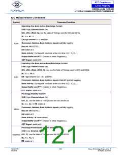
IDD Measurement Conditions
Symbol
Parameter/Condition
Operating One Bank Active-Precharge Current
CKE: High; External clock: On;
tCK, nRC, nRAS, CL: see the table of Timings used for IDD and IDDQ;
BL: 8(1); AL: 0;
:High between ACT and PRE;
Command, Address, Bank Address Inputs: partially toggling;
Data IO: MID-LEVEL;
IDD0
DM:stable at 0;
Bank Activity: Cycling with one bank active at a time: 0,0,1,1,2,2,...;
Output Buffer and RTT: Enabled in Mode Registers(2);
ODT Signal: stable at 0;
Operating One Bank Active-Read-Precharge Current
CKE: High; External clock: On;
tCK, nRC, nRAS, nRCD, CL: see see the table of Timings used for IDD and IDDQ;
BL: 8(1,7); AL:0;
: High between ACT, RD and PRE;
Command, Address, Bank Address Inputs, Data IO: partially toggling;
Bank Activity: Cycling with one bank active at a time: 0,0,1,1,2,2,...;
Output Buffer and RTT: Enabled in Mode Registers(2);
ODT Signal: stable at 0;
IDD1
Precharge Standby Current
CKE: High; External clock: On;
tCK, CL: see the table of Timings used for IDD and IDDQ;
BL: 8(1); AL: 0; : stable at 1;
Command, Address, Bank Address Inputs: partially toggling;
Data IO: MID-LEVEL;
IDD2N
DM:stable at 0;
Bank Activity: all banks closed;
Output Buffer and RTT: Enabled in Mode Registers(2);
ODT Signal: stable at 0;
Precharge Power-Down Current Slow Exit
CKE: Low; External clock: On;
tCK, CL: see the table of Timings used for IDD and IDDQ;
BL: 8(1); AL: 0;
IDD2P(0)
: stable at 1;
Version 1.4
05/2019
121
Nanya Technology Cooperation ©
All Rights Reserved.

 NANYA [ Nanya Technology Corporation. ]