NTC Proprietary
Level: Property
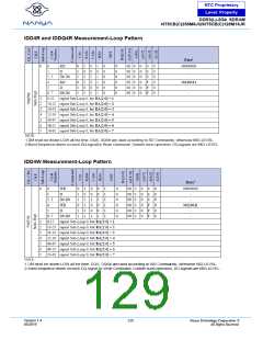
DDR3(L)-2Gb SDRAM
NT5CB(C)256M8JQ/NT5CB(C)128M16JR
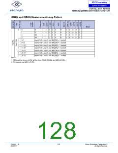
CKE: Low; External clock: Off; CK and : LOW; CL: see the table of Timings used for IDD and IDDQ;
BL: 8(1);AL: 0;
, Command, Address, Bank Address, Data IO: MID-LEVEL;
DM:stable at 0;
Bank Activity:Auto Self-Refresh operation;
Output Buffer and RTT: Enabled in Mode Registers(2);
ODT Signal: MIDLEVEL
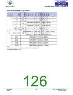
Operating Bank Interleave Read Current
CKE: High; External clock: On;
tCK, nRC, nRAS, nRCD, nRRD, nFAW, CL: see the table of Timings used for IDD and IDDQ;
BL: 8(1,7); AL: CL-1;
: High between ACT and RDA;
Command, Address, Bank Address Inputs:partially toggling;
Data IO: read data bursts with different data between one burst and the next one;
DM:stable at 0;
IDD7
Bank Activity: two times interleaved cycling through banks (0, 1, ...7) with different addressing;
Output Buffer and RTT: Enabled in Mode Registers(2);
ODT Signal: stable at 0;
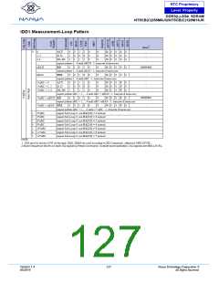
RESET Low Current
RESET: LOW; External clock: Off;
CK and : LOW; CKE: FLOATING;
IDD8
, Command, Address,Bank Address, Data IO: FLOATING;
ODT Signal: FLOATING
RESET Low current reading is valid once power is stable and RESET has been LOW for at least 1ms.
NOTE 1. Burst Length: BL8 fixed by MRS: set MR0 A[1,0]=00B
NOTE 2. Output Buffer Enable: set MR1 A[12] = 0B; set MR1 A[5,1] = 01B; RTT_Nom enable: set MR1 A[9,6,2] = 011B; RTT_Wr
enable: set MR2 A[10,9] = 10B
NOTE 3. Pecharge Power Down Mode: set MR0 A12=0B for Slow Exit or MR0 A12=1B for Fast Exit
NOTE 4. Auto Self-Refresh (ASR): set MR2 A6 = 0B to disable or 1B to enable feature
NOTE 5. Self-Refresh Temperature Range (SRT): set MR2 A7=0B for normal or 1B for extended temperature range
NOTE 6. Refer to DRAM supplier data sheet and/or DIMM SPD to determine if optional features or requirements are supported by
DDR3 SDRAM device
NOTE 7. Read Burst Type: Nibble Sequential, set MR0 A[3] = 0B
Version 1.4
05/2019
125
Nanya Technology Cooperation ©
All Rights Reserved.

 NANYA [ Nanya Technology Corporation. ]