Freescale Semiconductor, Inc.
Appendix: 68HC912D60A Flash EEPROM
Flash EEPROM Registers
22.6 Flash EEPROM Registers
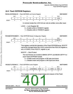
FEE32LCK/FEE28LCK — Flash EEPROM Lock Control Register
$00F4/$00F8
Bit 7
6
0
0
5
0
0
4
0
0
3
0
0
2
0
0
1
0
0
Bit 0
LOCK
0
0
0
RESET:
In normal modes the LOCK bit can only be written once after reset.
LOCK — Lock Register Bit
0 = Enable write to FEEMCR register
1 = Disable write to FEEMCR register
FEE32MCR/FEE28MCR — Flash EEPROM Module Configuration Register
$00F5/$00F9
Bit 7
6
0
0
5
0
0
4
0
0
3
0
0
2
0
0
1
0
0
Bit 0
0
0
BOOTP
1
RESET:
This register controls the operation of the Flash EEPROM array. BOOTP
cannot be changed when the LOCK control bit in the FEELCK register is
set or if ENPE in the FEECTL register is set.
BOOTP — Boot Protect
The boot blocks are located at $6000–$7FFF and $E000–$FFFF for
each Flash EEPROM module.
0 = Enable erase and program of 8K byte boot block
1 = Disable erase and program of 8K byte boot block
FEE32CTL/FEE28CTL — Flash EEPROM Control Register
$00F7/$00FB
Bit 7
6
0
0
5
0
0
4
FEESWAI
0
3
HVEN
0
2
0
0
1
ERAS
0
Bit 0
PGM
0
0
0
RESET:
This register controls the programming and erasure of the Flash
EEPROM.
68HC(9)12D60 — Rev 4.0
MOTOROLA
Advance Information
401
Appendix: 68HC912D60A Flash EEPROM
For More Information On This Product,
Go to: www.freescale.com

 MOTOROLA [ MOTOROLA ]