Freescale Semiconductor, Inc.
Appendix: 68HC912D60A Flash EEPROM
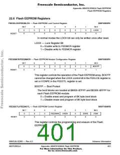
FEESWAI — Flash EEPROM Stop in Wait Control
0 = Do not halt Flash EEPROM clock when the part is in wait
mode.
1 = Halt Flash EEPROM clock when the part is in wait mode.
HVEN — High-Voltage Enable
This bit enables the charge pump to supply high voltages for program
and erase operations in the array. HVEN can only be set if either PGM
or ERAS are set and the proper sequence for program or erase is
followed.
0 = Disables high voltage to array and charge pump off
1 = Enables high voltage to array and charge pump on
ERAS — Erase Control
This bit configures the memory for erase operation. ERAS is
interlocked with the PGM bit such that both bits cannot be equal to 1
or set to1 at the same time.
0 = Erase operation is not selected.
1 = Erase operation selected.
PGM — Program Control
This bit configures the memory for program operation. PGM is
interlocked with the ERAS bit such that both bits cannot be equal to 1
or set to1 at the same time.
0 = Program operation is not selected.
1 = Program operation selected.
Advance Information
402
68HC(9)12D60 — Rev 4.0
Appendix: 68HC912D60A Flash EEPROM
MOTOROLA
For More Information On This Product,
Go to: www.freescale.com

 MOTOROLA [ MOTOROLA ]