Freescale Semiconductor, Inc.
Motorola Interconnect Bus
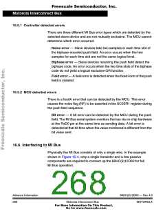
Interfacing to MI Bus
VDD
+12V
1.2kΩ
4.7kΩ
18V
MI Bus
VDD
T1
TX
3.9kΩ
VDD
10kΩ
MCU
22kΩ
10kΩ
RX
VSS
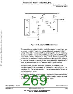
Figure 16-4. A typical MI Bus interface
The transistor serves both to drive the MI Bus during the push field and
to protect the MCU TX pin from voltage transients generated in the
wiring. Without the transistor, EMI could damage the TX pin. Similarly,
the input pin (RX) is protected from EMI by clamping it to the MCU supply
rails with two diodes. When a load dump occurs, the zener diode (18V)
is switched on and hence turns the transistor on; this generates the logic
‘0’ state on the MI Bus. After eight time slots (200ms) of continuous ‘0’
state, all devices on the MI Bus will have their outputs disabled.
The MI Bus line can take two states, recessive or dominant. The
dominant state (‘0’) is represented by a maximum 0.3V (V
of the
CESAT
transistor, T1). The recessive state (‘1’) is represented by 5V, through a
pull-up resistor of 10kΩ.
The bus load depends on the number of devices on the bus. Each device
has a pull-up resistor of 10kΩ. An external termination resistor is used
to stabilize the load resistance of the bus at 600Ω.
68HC(9)12D60 — Rev 4.0
MOTOROLA
Advance Information
Motorola Interconnect Bus
269
For More Information On This Product,
Go to: www.freescale.com

 MOTOROLA [ MOTOROLA ]