Freescale Semiconductor, Inc.
Motorola Interconnect Bus
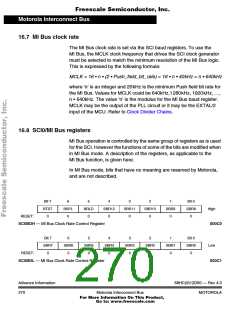
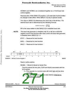
SCI0/MI Bus registers
SC0BDH and SC0BDL are considered together as a 16-bit baud rate
control register.
Read any time. Write SBR[12:0] anytime. Low order byte must be written
for change to take effect. Write SBR[15:13] only in special modes.
The value in SBR[12:0] determines the clock rate of the MI Bus. The
desired baud rate is determined by the following formula:
MCLK
MI BUS Clock Rate = --------------------
16 × BR
BR is the value written to bits SBR[12:0] to establish baud rate.
NOTE: The baud rate generator is disabled until TE or RE bit in SC0CR2
register is set for the first time after reset, and/or the baud rate generator
is disabled when SBR[12:0] = 0.
BTST — Reserved for test function
BSPL — Reserved for test function
BRLD — Reserved for test function
Bit 7
—
6
WOMS
0
5
—
0
4
—
0
3
—
0
2
—
0
1
—
0
Bit 0
PT
0
RESET:
0
SC0CR1 — MI Bus Control Register 1
$00C2
Read or write anytime.
WOMS — Wired-Or Mode for Serial Pins
This bit controls the two pins (TxD0 and RxD0) associated with the
SC0 section.
0 = Pins operate in a normal mode with both high and low drive
capability.
1 = Each pin operates in an open drain fashion if that pin is
declared as an output.
68HC(9)12D60 — Rev 4.0
MOTOROLA
Advance Information
Motorola Interconnect Bus
271
For More Information On This Product,
Go to: www.freescale.com

 MOTOROLA [ MOTOROLA ]