Freescale Semiconductor, Inc.
Motorola Interconnect Bus
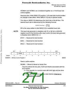
PT — MI Bus TxD0 polarity
If parity is enabled, this bit determines even or odd parity for both the
receiver and the transmitter.
0 = MI Bus transmit pin functions normally.
1 = MI Bus transmit pin will send inverted data.
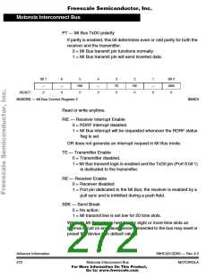
Bit 7
—
6
—
0
5
RIE
0
4
—
0
3
TE
0
2
RE
0
1
—
0
Bit 0
SBK
0
RESET:
0
SC0CR2 — MI Bus Control Register 2
$00C3
Read or write anytime.
RIE — Receiver Interrupt Enable
0 = RDRF interrupt disabled.
1 = MI Bus interrupt will be requested whenever the RDRF status
flag is set.
OR does not generate an interrupt request in MI Bus mode.
TE — Transmitter Enable
0 = Transmitter disabled.
1 = MI Bus transmit logic is enabled and the TxD0 pin (Port S bit 1)
is dedicated to the transmitter.
RE — Receiver Enable
0 = Receiver disabled.
1 = Port pin dedicated to the MI Bus; the receiver is enabled by a
pull sync and is inhibited during a push field.
SBK — Send Break
0 = No action.
1 = MI transmit line is set low for 20 time slots.
When an MI Bus wire is held low for eight or more time slots an
internal circuit on any slave device connected to the bus may reset or
preset the device with default values.
Advance Information
272
68HC(9)12D60 — Rev 4.0
Motorola Interconnect Bus
MOTOROLA
For More Information On This Product,
Go to: www.freescale.com

 MOTOROLA [ MOTOROLA ]