Freescale Semiconductor, Inc.
Multiple Serial Interface
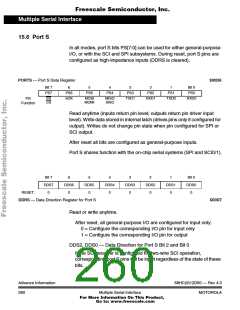
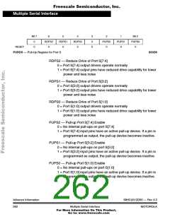
Port S
DDS3, DDS1 — Data Direction for Port S Bit 3 and Bit 1
If the SCI transmitter is configured for two-wire SCI operation,
corresponding port S pins will be output regardless of the state of
these bits.
DDS[6:4] — Data Direction for Port S Bits 6 through 4
If the SPI is enabled and expects the corresponding port S pin to be
an input, it will be an input regardless of the state of the DDRS bit. If
the SPI is enabled and expects the bit to be an output, it will be an
output ONLY if the DDRS bit is set.
DDS7 — Data Direction for Port S Bit 7
In SPI slave mode, DDRS7 has no meaning or effect; the PS7 pin is
dedicated as the SS input. In SPI master mode, DDRS7 determines
whether PS7 is an error detect input to the SPI or a general-purpose
or slave select output line.
NOTE: If mode fault error occurs, bits 5, 6 and 7 are forced to zero.
68HC(9)12D60 — Rev 4.0
MOTOROLA
Advance Information
261
Multiple Serial Interface
For More Information On This Product,
Go to: www.freescale.com

 MOTOROLA [ MOTOROLA ]