Freescale Semiconductor, Inc.
Multiple Serial Interface
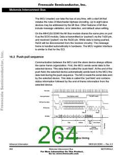
15.6 Port S
In all modes, port S bits PS[7:0] can be used for either general-purpose
I/O, or with the SCI and SPI subsystems. During reset, port S pins are
configured as high-impedance inputs (DDRS is cleared).
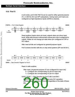
PORTS — Port S Data Register
$00D6
Bit 7
PS7
6
5
4
3
2
1
Bit 0
PS0
PS6
SCK
PS5
PS4
PS3
TXD1
PS2
RXD1
PS1
TXD0
Pin
Function
SS
CS
MOSI
MOMI
MISO
SISO
RXD0
Read anytime (inputs return pin level; outputs return pin driver input
level). Write data stored in internal latch (drives pins only if configured for
output). Writes do not change pin state when pin configured for SPI or
SCI output.
After reset all bits are configured as general-purpose inputs.
Port S shares function with the on-chip serial systems (SPI and SCI0/1).
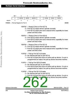
Bit 7
DDS7
0
6
DDS6
0
5
DDS5
0
4
DDS4
0
3
DDS3
0
2
DDS2
0
1
DDS1
0
Bit 0
DDS0
0
RESET:
DDRS — Data Direction Register for Port S
$00D7
Read or write anytime.
After reset, all general-purpose I/O are configured for input only.
0 = Configure the corresponding I/O pin for input only
1 = Configure the corresponding I/O pin for output
DDS2, DDS0 — Data Direction for Port S Bit 2 and Bit 0
If the SCI receiver is configured for two-wire SCI operation,
corresponding port S pins will be input regardless of the state of these
bits.
Advance Information
260
68HC(9)12D60 — Rev 4.0
Multiple Serial Interface
MOTOROLA
For More Information On This Product,
Go to: www.freescale.com

 MOTOROLA [ MOTOROLA ]