Freescale Semiconductor, Inc.
Multiple Serial Interface
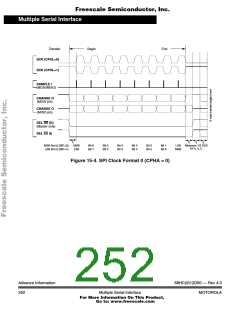
CPOL, CPHA — SPI Clock Polarity, Clock Phase
These two bits are used to specify the clock format to be used in SPI
operations. When the clock polarity bit is cleared and data is not being
transferred, the SCK pin of the master device is low. When CPOL is
set, SCK idles high. See Figure 15-4 and Figure 15-5.
SSOE — Slave Select Output Enable
The SS output feature is enabled only in the master mode by
asserting the SSOE and DDS7.
LSBF — SPI LSB First enable
0 = Data is transferred most significant bit first
1 = Data is transferred least significant bit first
Normally data is transferred most significant bit first.This bit does not
affect the position of the MSB and LSB in the data register. Reads and
writes of the data register will always have MSB in bit 7.
Bit 7
6
0
0
5
0
0
4
0
0
3
0
0
2
0
0
1
SPSWAI
0
Bit 0
SPC0
0
0
0
RESET:
SP0CR2 — SPI Control Register 2
$00D1
Read or write anytime.
SPSWAI — Serial Interface Stop in WAIT mode
0 = Serial interface clock operates normally
1 = Halt serial interface clock generation in WAIT mode
Advance Information
256
68HC(9)12D60 — Rev 4.0
MOTOROLA
Multiple Serial Interface
For More Information On This Product,
Go to: www.freescale.com

 MOTOROLA [ MOTOROLA ]