Freescale Semiconductor, Inc.
Enhanced Capture Timer
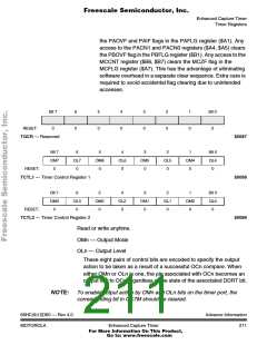
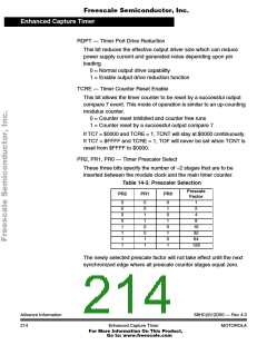
Table 14-1. Compare Result Output Action
OMn
OLn
Action
0
0
1
1
0
1
0
1
Timer disconnected from output pin logic
Toggle OCn output line
Clear OCn output line to zero
Set OCn output line to one
To operate the 16-bit pulse accumulators A and B (PACA and PACB)
independently of input capture or output compare 7 and 0 respectively
the user must set the corresponding bits IOSn = 1, OMn = 0 and OLn
= 0. OC7M7 or OC7M0 in the OC7M register must also be cleared.
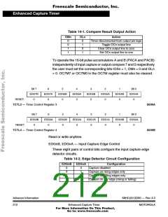
Bit 7
EDG7B
0
6
EDG7A
0
5
EDG6B
0
4
EDG6A
0
3
EDG5B
0
2
EDG5A
0
1
EDG4B
0
Bit 0
EDG4A
0
RESET:
TCTL3 — Timer Control Register 3
$008A
$008B
Bit 7
EDG3B
0
6
EDG3A
0
5
EDG2B
0
4
EDG2A
0
3
EDG1B
0
2
EDG1A
0
1
EDG0B
0
Bit 0
EDG0A
0
RESET:
TCTL4 — Timer Control Register 4
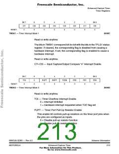
Read or write anytime.
EDGnB, EDGnA — Input Capture Edge Control
These eight pairs of control bits configure the input capture edge
detector circuits.
Table 14-2. Edge Detector Circuit Configuration
EDGnB
EDGnA
Configuration
Capture disabled
0
0
1
1
0
1
0
1
Capture on rising edges only
Capture on falling edges only
Capture on any edge (rising or falling)
Advance Information
212
68HC(9)12D60 — Rev 4.0
MOTOROLA
Enhanced Capture Timer
For More Information On This Product,
Go to: www.freescale.com

 MOTOROLA [ MOTOROLA ]