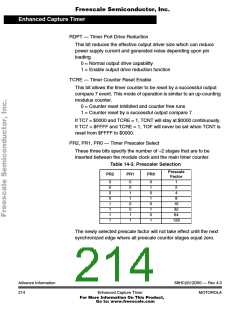
Freescale Semiconductor, Inc.
Enhanced Capture Timer
Timer Registers
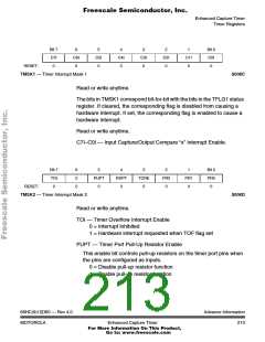
the PAOVF and PAIF flags in the PAFLG register ($A1). Any
access to the PACN1 and PACN0 registers ($A4, $A5) clears
the PBOVF flag in the PBFLG register ($B1). Any access to the
MCCNT register ($B6, $B7) clears the MCZF flag in the
MCFLG register ($A7). This has the advantage of eliminating
software overhead in a separate clear sequence. Extra care is
required to avoid accidental flag clearing due to unintended
accesses.
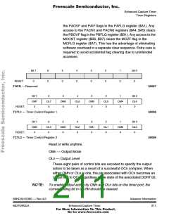
Bit 7
0
6
0
5
0
4
0
3
0
2
0
1
0
Bit 0
0
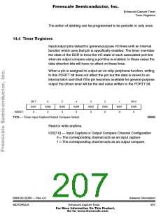
RESET:
TQCR — Reserved
$0087
$0088
$0089
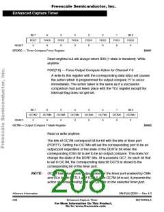
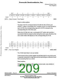
Bit 7
OM7
6
5
4
3
2
1
OM4
0
Bit 0
OL4
0
OL7
0
OM6
0
OL6
0
OM5
0
OL5
0
RESET:
0
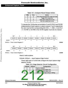
TCTL1 — Timer Control Register 1
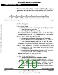
Bit 7
OM3
0
6
OL3
0
5
OM2
0
4
OL2
0
3
OM1
0
2
OL1
0
1
OM0
0
Bit 0
OL0
0
RESET:
TCTL2 — Timer Control Register 2
Read or write anytime.
OMn — Output Mode
OLn — Output Level
These eight pairs of control bits are encoded to specify the output
action to be taken as a result of a successful OCn compare. When
either OMn or OLn is one, the pin associated with OCn becomes an
output tied to OCn regardless of the state of the associated DDRT bit.
NOTE: To enable output action by OMn and OLn bits on the timer port, the
corresponding bit in OC7M should be cleared.
68HC(9)12D60 — Rev 4.0
MOTOROLA
Advance Information
211
Enhanced Capture Timer
For More Information On This Product,
Go to: www.freescale.com

 MOTOROLA [ MOTOROLA ]