Power Consumption Considerations
4.3 Power Consumption Considerations
Power dissipation is a key issue in portable DSP applications. Some of the factors affecting current
consumption are described in this section. Most of the current consumed by CMOS devices is alternating
current (ac), which is charging and discharging the capacitances of the pins and internal nodes.
Current consumption is described by this formula:
Equation 3: I = C × V × f
Where:
C
V
f
=
=
=
node/pin capacitance
voltage swing
frequency of node/pin toggle
Example 4-1. Current Consumption
For a Port A address pin loaded with 50 pF capacitance, operating at 3.3 V, with a 66 MHz clock, toggling at its
maximum possible rate (33 MHz), the current consumption is expressed in Equation 4.
Equation 4: I = 50 × 10–12 × 3.3 × 33 × 106 = 5.48 mA
The maximum internal current (I max) value reflects the typical possible switching of the internal
CCI
buses on best-case operation conditions—not necessarily a real application case. The typical internal
current (I
) value reflects the average switching of the internal buses on typical operating conditions.
CCItyp
Perform the following steps for applications that require very low current consumption:
1.
2.
3.
4.
5.
6.
7.
Set the EBD bit when you are not accessing external memory.
Minimize external memory accesses, and use internal memory accesses.
Minimize the number of pins that are switching.
Minimize the capacitive load on the pins.
Connect the unused inputs to pull-up or pull-down resistors.
Disable unused peripherals.
Disable unused pin activity (for example, CLKOUT, XTAL).
One way to evaluate power consumption is to use a current-per-MIPS measurement methodology to
minimize specific board effects (that is, to compensate for measured board current not caused by the
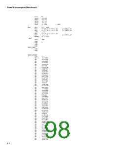
DSP). A benchmark power consumption test algorithm is listed in Appendix A. Use the test algorithm,
specific test current measurements, and the following equation to derive the current-per-MIPS value.
Equation 5: I ⁄ MIPS = I ⁄ MHz = (ItypF2 – ItypF1) ⁄ (F2 – F1)
Where:
I
I
=
=
current at F2
current at F1
typF2
typF1
F2
F1
=
=
high frequency (any specified operating frequency)
low frequency (any specified operating frequency lower than F2)
Note: F1 should be significantly less than F2. For example, F2 could be 66 MHz and F1 could be 33
MHz. The degree of difference between F1 and F2 determines the amount of precision with
which the current rating can be determined for an application.
4-4

 MOTOROLA [ MOTOROLA ]