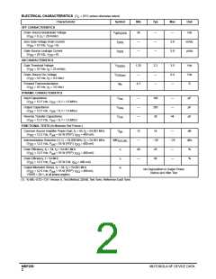
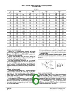
GATE CHARACTERISTICS
The gate of the RF MOSFET is a polysilicon material, and
is electrically isolated from the source by a layer of oxide.
on the drain are both high, then the signal coupled to the gate
may be large enough to exceed the gate–threshold voltage
and turn the device on.
9
The input resistance is very high — on the order of 10 ohms
DC BIAS
— resulting in a leakage current of a few nanoamperes.
Gate control is achieved by applying a positive voltage to
the gate greater than the gate–to–source threshold voltage,
Since the MRF255 is an enhancement mode FET, drain
current flows only when the gate is at a higher potential than
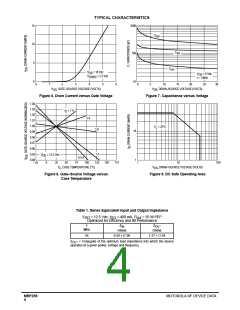
the source. See Figure 8 for a typial plot of drain current ver-
sus gate voltage. RF power FETs operate optimally with a
V
.
GS(th)
Gate Voltage Rating — Never exceed the gate voltage
rating. Exceeding the rated V can result in permanent
quiescent drain current (I
), whose value is application de-
DQ
pendent. The MRF255 was characterized for linear and CW
operation at I = 400 mA, which is the suggested value of
GS
damage to the oxide layer in the gate region.
DQ
Gate Termination — The gates of these devices are
essentially capacitors. Circuits that leave the gate open–
circuited or floating should be avoided. These conditions can
result in turn–on of the devices due to voltage build–up on
the input capacitor due to leakage currents or pickup.
Gate Protection — These devices do not have an internal
monolithic zener diode from gate–to–source. If gate protec-
tion is required, an external zener diode is recommended.
Using a resistor to keep the gate–to–source impedance
low also helps damp transients and serves another important
function. Voltage transients on the drain can be coupled to
the gate through the parasitic gate–drain capacitance. If the
gate–to–source impedance and the rate of voltage change
bias current for typical applications.
The gate is a dc open circuit and draws essentially no cur-
rent. Therefore, the gate bias circuit may generally be just a
simple resistive divider network. Some applications may re-
quire a more elaborate bias sytem.
GAIN CONTROL
For CW applications, power output of the MRF255 may be
controlled to some degree with a low power dc control signal
applied to the gate, thus facilitating applications such as
manual gain control, AGC/ALC and modulation systems.
The characteristic is very dependent on frequency and load
line.
MOTOROLA RF DEVICE DATA
MRF255
7

 MOTOROLA [ MOTOROLA ]