Table 2. Common Source Scattering Parameters (continued)
(V = 12.5 Vdc)
DS
I
D
= 1 A
S
11
S
21
S
12
S
22
f
(MHz)
|S
|
φ
|S
|
φ
152
133
110
99
92
89
86
84
82
80
78
76
74
71
68
65
62
59
56
53
51
|S
|
φ
|S
|
φ
–162
–163
–170
–175
–178
–179
–180
180
11
21
12
22
1
0.98
0.96
0.93
0.93
0.92
0.92
0.92
0.92
0.92
0.92
0.92
0.92
0.92
0.92
0.92
0.92
0.92
0.92
0.92
0.92
0.92
–54
65.5
50.9
26.2
13.7
6.96
4.65
3.49
2.79
2.32
1.99
1.74
1.54
1.39
1.15
0.98
0.86
0.76
0.68
0.61
0.56
0.51
0.006
0.009
0.011
0.012
0.012
0.012
0.013
0.013
0.013
0.014
0.014
0.015
0.016
0.017
0.019
0.020
0.022
0.024
0.026
0.028
0.030
63
0.60
0.75
0.88
0.91
0.92
0.93
0.93
0.93
0.93
0.93
0.93
0.93
0.93
0.93
0.93
0.93
0.93
0.94
0.94
0.94
0.94
2
–91
44
23
15
15
18
21
25
28
31
34
37
40
44
48
51
54
56
58
59
61
5
–137
–158
–169
–173
–175
–176
–177
–178
–179
–179
–180
180
10
20
30
40
50
60
179
70
179
80
179
90
178
100
120
140
160
180
200
220
240
260
178
177
179
177
178
176
178
176
177
175
177
175
176
174
176
173
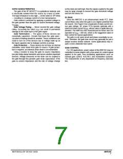
DESIGN CONSIDERATIONS
1. Drain shorted to source and positive voltage at the gate.
The MRF255 is a common–surce, RF power, N–channel
enhancement mode Metal–Oxide Semiconductor Field–Effect
Transistor (MOSFET). Motorola RF MOSFETs feature a verti-
cal structure with a planar design.
Motorola Application Note AN211A, FETs in Theory and
Practice, is suggested reading for those not familiar with the
construction and characteristics of FETs.
2. Positivevoltageofthedraininrespecttosourceandzero
volts at the gate.
In the latter case the numbers are lower. However, neither
method represents the actual operating conditions in RF ap-
plications.
This device was designed primarily for HF 12.5 V mobile
linear power amplifier applications. The major advantages of
RF power MOSFETs include high gain, simple bias systems,
relative immunity from thermal runaway, and the ability to
withstand severely mismatched loads without suffering dam-
age.
DRAIN
C
gd
GATE
C
C
C
= C + C
gd gs
iss
C
= C + C
ds
oss
rss
gd ds
= C
gd
C
gs
SOURCE
MOSFET CAPACITANCES
The physical structure of a MOSFET results in capacitors
between all three terminals. The metal oxide gate structure
determines the capacitors from gate–to–drain (C ), and
DRAIN CHARACTERISTICS
One critical figure of merit for a FET is its static resistance
inthefull–oncondition. Thison–resistance, R , occurs
in the linear region of the output characteristic and is speci-
fied at a specific gate–source voltage and drain current. The
drain–source voltage under these conditions is termed
gd
gate–to–source (C ). The PN junction formed during fab-
gs
rication of the RF MOSFET results in a junction capacitance
DS(on)
from drain–to–source (C ).
ds
These capacitances are characterized as input (C ), output
iss
(C ) and reverse transfer (C ) capacitances on data sheets.
oss rss
The relationships between the inter–terminal capacitances and
V
ForMOSFETs,V
hasapositivetemperature
DS(on).
DS(on)
those given on data sheets are shown below. The C
be specified in two ways:
can
coefficient at high temperatures because it contributes to
the power dissipation within the device.
iss
MRF255
6
MOTOROLA RF DEVICE DATA

 MOTOROLA [ MOTOROLA ]