MC1377
ELECTRICAL CHARACTERISTICS (V
= 12 Vdc, T = 25°C, circuit of Figure 7, unless otherwise noted.)
A
CC
Characteristics
Pins
Symbol
Min
Typ
Max
Unit
VIDEO INPUT
R, G, B Input DC Levels
3, 4, 5
RGB
2.8
–
3.3
1.0
3.8
–
Vdc
R, G, B Input for 100% Color Saturation
V
pp
R, G, B Input: Resistance
R, G, B Input: Capacitance
R
C
8.0
–
10
2.0
17
–
kΩ
pF
RGB
RGB
Sync Input Resistance (1.7 V < Input < 8.2)
2
9
Sync
–
10
–
kΩ
COMPOSITE VIDEO OUTPUT
CV
out
–
–
–
–
0.6
1.4
1.7
0.6
–
–
–
–
V
pp
Sync
Composite Output,
100% Saturation
(see Figure 8d)
Luminance
Chroma
Burst
Ω
Output Impedance (Note 1)
R
–
–
50
20
–
–
video
Subcarrier Leakage in Output (Note 2)
V
lk
mV
pp
NOTES: 1. Output Impedance can be reduced to less than 10 Ω by using a 150 Ω output load from Pin 9 to ground. Power supply current will
increase to about 60 mA.
2. Subcarrier leakage can be reduced to less than 10 mV with optional circuitry (see Figure 12).
PIN FUNCTION DESCRIPTIONS
Symbol
Pin
1
Description
t
r
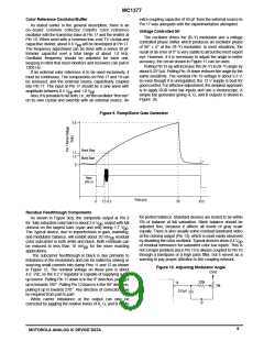
External components at this pin set the rise time of the internal ramp function generator (see Figure 10).
Sync
R
2
Composite sync input. Presents 10 kΩ resistance to input.
3
Red signal input. Presents 10 kΩ impedance to input. 1.0 V required for 100% saturation.
pp
G
4
Green signal input. Presents 10 kΩ impedance to input. 1.0 V
pp required for 100% saturation.
B
5
Blue signal Input. Presents 10 kΩ impedance to input. 1.0 V
pp required for 100% saturation.
–Y
out
6
Luma (–Y) output. Allows external setting of luma delay time.
V
7
Video Clamp pin. Typical connection is a 0.01 µF capacitor to ground.
Luma (–Y) input. Presents 10 kΩ input impedance.
Composite Video output. 50 Ω output impedance.
clamp
–Y
in
8
CV
out
9
Chroma
10
11
Chroma input. Presents 10 kΩ input impedance.
In
B–Y
B–Y clamp. Clamps B–Y during blanking with a 0.1 µF capacitor to ground.
Also used with R–Y clamp to null residual color subcarrier in output.
clamp
R–Y
12
R–Y clamp. Clamps R–Y during blanking with a 0.1 µF capacitor to ground.
Also used with B–Y clamp to null residual color subcarrier in output.
clamp
Chroma
Out
13
14
15
16
17
Chroma output. 50 Ω output impedance.
V
CC
Power supply pin for the IC; +12, ± 2.0 V, required at 35 mA (typical).
Ground pin.
Gnd
V
B
8.2 V reference from an internal regulator capable of delivering 10 mA to external circuitry.
Osc
Oscillator input. A transistor base presents 5.0 kΩ to an external subcarrier input, or is available for
constructing a Colpitts oscillator (see Figure 4).
in
Osc
18
19
20
Oscillator output. The emitter of the transistor, with base access at Pin 17, is accessible for completing the
Colpitts oscillator. See Figure 4.
out
Quad decoupler. With external circuitry, R–Y to B–Y relative angle errors can be corrected. Typically,
requires a 0.01 µF capacitor to ground.
m
NTSC/PAL
Select
NTSC/PAL switch. When grounded, the MC1377 is in the NTSC mode; if unconnected, in the PAL mode.
3
MOTOROLA ANALOG IC DEVICE DATA

 MOTOROLA [ MOTOROLA ]