Ver. 1.1
MITSUBISHI LSIs
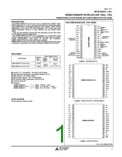
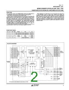
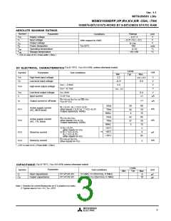
M5M51008DFP,VP,RV,KV,KR -55H, -70H
1048576-BIT(131072-WORD BY 8-BIT)CMOS STATIC RAM
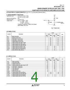
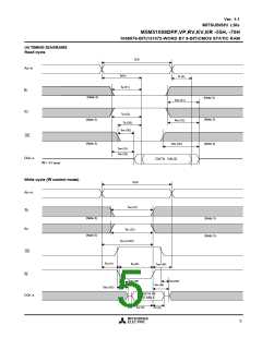
Write cycle ( S1 control mode)
tCW
A0~16
tsu (A)
trec (W)
tsu (S1)
S1
S2
(Note 3)
(Note 3)
(Note 3)
(Note 5)
W
(Note 4)
(Note 3)
th (D)
tsu (D)
DATA IN
STABLE
DQ1~8
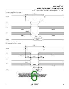
Write cycle (S2 control mode)
tCW
A0~16
S1
(Note 3)
(Note 3)
tsu (A)
tsu (S2)
trec (W)
S2
W
(Note 5)
(Note 4)
(Note 3)
(Note 3)
tsu (D)
th (D)
DATA IN
STABLE
DQ1~8
Note 3: Hatching indicates the state is "don't care".
4: Writing is executed while S2 high overlaps S1 and W low.
5: When the falling edge of W is simultaneously or prior to the falling edge of S1
or rising edge of S2, the outputs are maintained in the high impedance state.
6: Don't apply inverted phase signal externally when DQ pin is output mode.
MITSUBISHI
ELECTRIC
6

 MITSUBISHI [ Mitsubishi Group ]