Ver. 1.1
MITSUBISHI LSIs
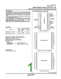
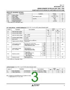
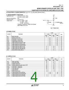
M5M51008DFP,VP,RV,KV,KR -55H, -70H
1048576-BIT(131072-WORD BY 8-BIT)CMOS STATIC RAM
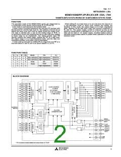
FUNCTION
The operation mode of the M5M51008D series are determined by
a combination of the device control inputs S1,S2,W and OE.
Each mode is summarized in the function table.
When setting S1 at a high level or S2 at a low level, the chip are in
a non-selectable mode in which both reading and writing are
disabled. In this mode, the output stage is in a high- impedance
state, allowing OR-tie with other chips and memory expansion by
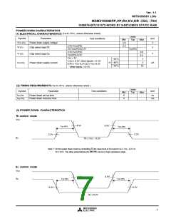
S1 and S2. The power supply current is reduced as low as the
stand-by current which is specified as ICC3 or ICC4, and the memory
data can be held at +2V power supply, enabling battery back-up
operation during power failure or power-down operation in the non-
selected mode.
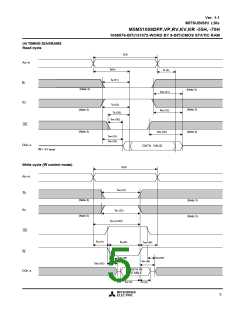
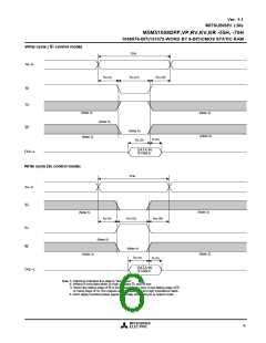
A write cycle is executed whenever the low level W overlaps with
the low level S1 and the high level S2. The address must be set up
before the write cycle and must be stable during the entire cycle.
The data is latched into a cell on the trailing edge of W,S1 or
S2,whichever occurs first,requiring the set-up and hold time relative
to these edge to be maintained. The output enable input OE
directly controls the output stage. Setting the OE at a high level,
the output stage is in a high-impedance state, and the data bus
contention problem in the write cycle is eliminated.
A read cycle is executed by setting W at a high level and OE at a
low level while S1 and S2 are in an active state(S1=L,S2=H).
FUNCTION TABLE
Mode
DQ
ICC
S1 S2
W
X
X
L
OE
X
X
H
L
L
Stand-by
Non selection High-impedance
X
H
X
Non selection High-impedance Stand-by
Din
Dout
Active
Active
Active
X
Write
Read
L
L
H
H
H
H
L
H
High-impedance
BLOCK DIAGRAM
*
*
DQ1
13
14
15
21
22
23
A3
9
17
18
15
DQ2
DQ3
A2 10
131072 WORDS
X 8 BITS
(512 ROWS
X128 COLUMNS
X 16BLOCKS)
A5
7
DATA
INPUTS/
OUTPUTS
17
18
19
25
26
27
DQ4
DQ5
DQ6
A6
A7
6
5
14
13
12
11
10
7
A12
A14
A16
A15
4
28
29
20 DQ7
21 DQ8
3
2
31
ADDRESS
INPUTS
CLOCK
GENERATOR
A13
A8
28
27
26
25
4
3
2
1
A9
A11
WRITE
CONTROL
INPUT
29
W
5
A4
8
16
19
20
31
30
6
22
30
S1
S2
CHIP
SELECT
INPUTS
A1 11
A0
12
A10 23
OUTPUT
ENABLE
INPUT
32
8
24 OE
32 VCC
GND
(0V)
16
24
* Pin numbers inside dotted line show those of TSOP
MITSUBISHI
ELECTRIC
2

 MITSUBISHI [ Mitsubishi Group ]