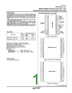
Ver. 1.1
MITSUBISHI LSIs
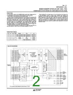
M5M51008DFP,VP,RV,KV,KR -55H, -70H
1048576-BIT(131072-WORD BY 8-BIT)CMOS STATIC RAM
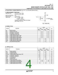
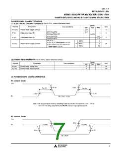
AC ELECTRICAL CHARACTERISTICS (Ta=0~70°C, 5V±10% unless otherwise noted )
(1) MEASUREMENT CONDITIONS
VCC
...............
Input pulse level
VIH=2.4V,VIL=0.6V (-70H)
VIH=3.0V,VIL=0.0V (-55H)
5ns
......
1.8kW
Input rise and fall time
................
Reference level
VOH=VOL=1.5V
DQ
.....................
Output loads
Fig.1, CL=100pF (-70H)
CL=30pF (-55H)
990W
CL ( Including scope
CL=5pF (for ten,tdis)
Transition is measured ± 500mV from steady
state voltage. (for ten,tdis)
and JIG )
Fig.1 Output load
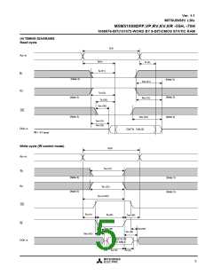
(2) READ CYCLE
Limits
-70H
Symbol
Parameter
-55H
Unit
Min
55
Max
Min
70
Max
tCR
Read cycle time
Address access time
ns
ns
ns
ns
ns
ns
ns
ns
ns
ns
ns
ns
ta(A)
55
55
55
30
20
20
20
70
70
70
35
25
25
25
ta(S1)
ta(S2)
ta(OE)
tdis(S1)
tdis(S2)
tdis(OE)
ten(S1)
Chip select 1 access time
Chip select 2 access time
Output enable access time
Output disable time after S1 high
Output disable time after S2 low
Output disable time after OE high
Output enable time after S1 low
Output enable time after S2 high
Output enable time after OE low
Data valid time after address
5
10
ten(S2)
ten(OE)
tV(A)
5
5
10
5
5
10
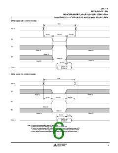
(3) WRITE CYCLE
Limits
Symbol
Parameter
-55H
-70H
Unit
Min
55
45
0
Max
Min
70
50
0
Max
ns
ns
ns
ns
ns
ns
ns
ns
ns
ns
ns
ns
ns
tCW
Write cycle time
Write pulse width
tw(W)
Address setup time
tsu(A)
tsu(A-WH)
tsu(S1)
tsu(S2)
tsu(D)
Address setup time with respect to W
Chip select 1 setup time
Chip select 2 setup time
Data setup time
50
50
50
25
0
55
55
55
30
0
th(D)
Data hold time
trec(W)
tdis(W)
tdis(OE)
ten(W)
ten(OE)
Write recovery time
0
0
20
20
25
25
Output disable time from W low
Output disable time from OE high
Output enable time from W high
Output enable time from OE low
5
5
5
5
MITSUBISHI
ELECTRIC
4

 MITSUBISHI [ Mitsubishi Group ]