MITSUBISHI MICROCOMPUTERS
3822 Group
SINGLE-CHIP 8-BIT CMOS MICROCOMPUTER
A-D CONVERTER
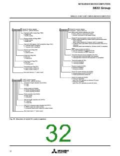
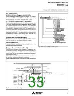
[A-D Conversion Register (AD)] 003516
The A-D conversion register is a read-only register that contains
the result of an A-D conversion. When reading this register during
an A-D conversion, the previous conversion result is read.
b7
b0
A-D control register
(ADCON : address 003416)
Analog input pin selection bits
0 0 0 : P60/AN0
0 0 1 : P61/AN1
0 1 0 : P62/AN2
[A-D Control Register (ADCON)] 003416
The A-D control register controls the A-D conversion process. Bits
0 to 2 of this register select specific analog input pins. Bit 3 signals
the completion of an A-D conversion. The value of this bit remains
at “0” during an A-D conversion, then changes to “1” when the A-
D conversion is completed. Writing “0” to this bit starts the A-D
conversion. Bit 4 controls the transistor which breaks the through
current of the resistor ladder. When bit 5, which is the AD external
trigger valid bit, is set to “1”, this bit enables A-D conversion even
by a falling edge of an ADT input. Set ports which share with ADT
pins to input when using an A-D external trigger.
0 1 1 : P63/AN3
1 0 0 : P64/AN4
1 0 1 : P65/AN5
1 1 0 : P66/AN6
1 1 1 : P67/AN7
AD conversion completion bit
0 : Conversion in progress
1 : Conversion completed
VREF input switch bit
0 : OFF
1 : ON
AD external trigger valid bit
0 : A-D external trigger invalid
1 : A-D external trigger valid
Interrupt source selection bit
0 : Interrupt request at A-D
conversion completed
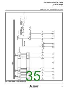
[Comparison Voltage Generator]
The comparison voltage generator divides the voltage between
AVSS and VREF by 256, and outputs the divided voltages.
1 : Interrupt request at ADT
input falling
Not used (returns “0” when read)
[Channel Selector]
The channel selector selects one of the input ports P67/AN7–P60/
AN0, and inputs it to the comparator.
Fig. 30 Structure of A-D control register
[Comparator and Control Circuit]
The comparator and control circuit compares an analog input volt-
age with the comparison voltage and stores the result in the A-D
conversion register. When an A-D conversion is completed, the
control circuit sets the AD conversion completion bit and the AD
interrupt request bit to “1”.
Note that the comparator is constructed linked to a capacitor, so
set f(XIN) to at least 500 kHz during A-D conversion.
Use the clock divided from the main clock XIN as the internal clock
φ.
Data bus
b7
b0
A-D control register
P57/ADT
3
ADT/A-D interrupt request
A-D control circuit
P60/AN0
P61/AN1
P62/AN2
P63/AN3
P64/AN4
P65/AN5
P66/AN6
P67/AN7
A-D conversion
register
Comparator
8
Resistor ladder
AVSS
VREF
Fig. 31 A-D converter block diagram
33

 MITSUBISHI [ Mitsubishi Group ]