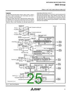
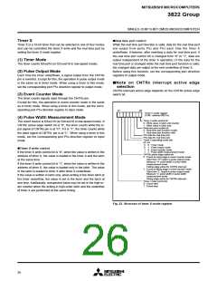
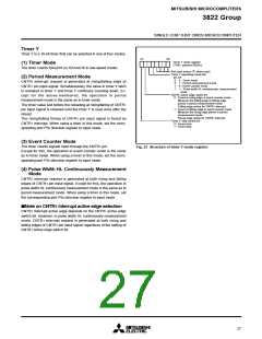
MITSUBISHI MICROCOMPUTERS
3822 Group
SINGLE-CHIP 8-BIT CMOS MICROCOMPUTER
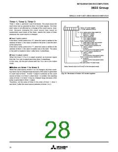
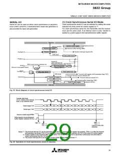
(1) Clock Synchronous Serial I/O Mode
Clock synchronous serial I/O can be selected by setting the mode
selection bit of the serial I/O control register to “1”.
SERIAL I/O
Serial I/O can be used as either clock synchronous or asynchro-
nous (UART) serial I/O. A dedicated timer (baud rate generator) is
also provided for baud rate generation.
For clock synchronous serial I/O, the transmitter and the receiver
must use the same clock. If an internal clock is used, transfer is
started by a write signal to the transmit/receive buffer register.
Data bus
Address 001A16
Receive buffer full flag (RBF)
Serial I/O control register
Address 001816
Receive buffer register
Receive shift register
Receive interrupt request (RI)
P44/RXD
Shift clock
Clock control circuit
P46/SCLK
Serial I/O
clock selection bit
Frequency division ratio 1/(n+1)
BRG count source selection bit
f(XIN
)
Baud rate generator
Address 001C16
1/4
(f(XCIN) in low-speed mode)
1/4
P47/SRDY1
Clock control circuit
Falling-edge detector
F/F
Shift clock
Transmit shift register shift completion flag (TSC)
Transmit interrupt source selection bit
P45/TXD
Transmit shift register
Transmit buffer register
Transmit interrupt request (TI)
Transmit buffer empty flag (TBE)
Address 001916
Serial I/O status register
Address 001816
Data bus
Fig. 25 Block diagram of clock synchronous serial I/O
Transfer shift clock
(1/2 to 1/2048 of the internal
clock, or an external clock)
D
0
0
D
1
1
D
2
D
3
3
D
4
4
D
5
5
D
6
6
D
7
7
Serial output T
XD
Serial input R
X
D
D
D
D
D
D
D
D
D
2
Receive enable signal SRDY
Write signal to receive/transmit
buffer register (address 001816
)
RBF = 1
TSC = 1
Overrun error (OE)
detection
TBE = 0
TBE = 1
TSC = 0
1 : The transmit interrupt (TI) can be generated either when the transmit buffer register has emptied (TBE=1) or after the transmit
shift operation has ended (TSC=1), by setting the transmit interrupt source selection bit (TIC) of the serial I/O control register.
2 : If data is written to the transmit buffer register when TSC=0, the transmit clock is generated continuously and serial data is
Notes
output continuously from the T
XD pin.
3 : The receive interrupt (RI) is set when the receive buffer full flag (RBF) becomes “1” .
Fig. 26 Operation of clock synchronous serial I/O function
29

 MITSUBISHI [ Mitsubishi Group ]