MITSUBISHI MICROCOMPUTERS
3822 Group
SINGLE-CHIP 8-BIT CMOS MICROCOMPUTER
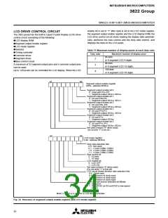
Table 12 Bias control and applied voltage to VL1–VL3
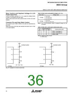
Bias Control and Applied Voltage to LCD
Power Input Pins
Bias value
Voltage value
To the LCD power input pins (VL1–VL3), apply the voltage shown
VL3=VLCD
in Table 12 according to the bias value.
1/3 bias
VL2=2/3 VLCD
VL1=1/3 VLCD
Select a bias value by the bias control bit (bit 2 of the LCD mode
register).
VL3=VLCD
1/2 bias
VL2=VL1=1/2 VLCD
Common Pin and Duty Ratio Control
The common pins (COM0–COM3) to be used are determined by
duty ratio.
Note 1: VLCD is the maximum value of supplied voltage for the
LCD panel.
Select duty ratio by the duty ratio selection bits (bits 0 and 1 of the
LCD mode register).
Table 13 Duty ratio control and common pins used
Duty ratio selection bit
Duty
Common pins used
ratio
Bit 1
Bit 0
2
3
4
0
1
1
1
0
1
COM0, COM1 (Note 1)
COM0–COM2 (Note 2)
COM0–COM3
Notes1: COM2 and COM3 are open.
2: COM3 is open.
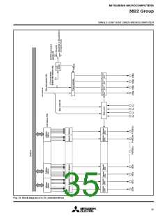
Contrast control
Contrast control
V
L3
V
L3
R1
R4
V
L2
V
L2
R2
R3
V
L1
V
L1
R5
R4 = R5
R1 = R2 = R3
1/3 bias
1/2 bias
Fig. 34 Example of circuit at each bias
36

 MITSUBISHI [ Mitsubishi Group ]