MITSUBISHI MICROCOMPUTERS
3822 Group
SINGLE-CHIP 8-BIT CMOS MICROCOMPUTER
enable bit is set to “1” after data is set in the LCD mode register,
the segment output enable register and the LCD display RAM, the
LCD drive control circuit starts reading the display data automati-
cally, performs the bias control and the duty ratio control, and
displays the data on the LCD panel.
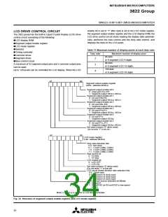
LCD DRIVE CONTROL CIRCUIT
The 3822 group has the built-in Liquid Crystal Display (LCD) drive
control circuit consisting of the following.
ꢀLCD display RAM
ꢀSegment output enable register
ꢀLCD mode register
ꢀSelector
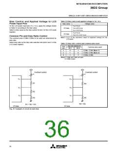
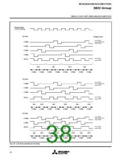
Table 11 Maximum number of display pixels at each duty ratio
ꢀTiming controller
Duty ratio
2
Maximum number of display pixel
64 dots
ꢀCommon driver
ꢀSegment driver
or 8 segment LCD 8 digits
96 dots
ꢀBias control circuit
A maximum of 32 segment output pins and 4 common output pins
can be used.
3
4
or 8 segment LCD 12 digits
128 dots
Up to 128 pixels can be controlled for LCD display. When the LCD
or 8 segment LCD 16 digits
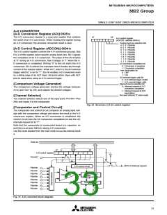
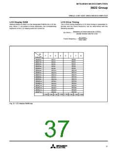
b7
b0
Segment output enable register
(SEG : address 003816
)
Segment output enable bit 0
0 : Input port P3 –P3
4
7
1 : Segment output SEG12–SEG15
Segment output enable bit 1
0 : I/O port P00,P01
1 : Segment output SEG16, SEG17
Segment output enable bit 2
0 : I/O port P02–P07
1 : Segment output SEG18–SEG23
Segment output enable bit 3
0 : I/O port P10,P11
1 : Segment output SEG24, SEG25
Segment output enable bit 4
0 : I/O port P1
2
1 : Segment output SEG26
Segment output enable bit 5
0 : I/O port P13–P17
1 : Segment output SEG27–SEG31
Not used (returns “0” when read)
(Do not write “1” to this bit.)
b7
b0
LCD mode register
(LM : address 003916
)
Duty ratio selection bits
0 0 : Not used
0 1 : 2 (use COM
1 0 : 3 (use COM
1 1 : 4 (use COM
Bias control bit
0 : 1/3 bias
0
0
0
, COM
–COM
–COM
1
2
3
)
)
)
1 : 1/2 bias
LCD enable bit
0 : LCD OFF
1 : LCD ON
Not used (returns “0” when read)
(Do not write “1” to this bit)
LCD circuit divider division ratio selection bits
0 0 : Clock input
0 1 : 2 division of clock input
1 0 : 4 division of clock input
1 1 : 8 division of clock input
LCDCK count source selection bit (Note)
0 : f(XCIN)/32
1 : f(XIN)/8192 (or f(XCIN)/8192 in low-speed
mode)
Note: LCDCK is a clock for a LCD timing controller.
Fig. 32 Structure of segment output enable register and LCD mode register
34

 MITSUBISHI [ Mitsubishi Group ]