Mitsubishi microcomputers
M16C / 62 Group
SINGLE-CHIP 16-BIT CMOS MICROCOMPUTER
Revision History
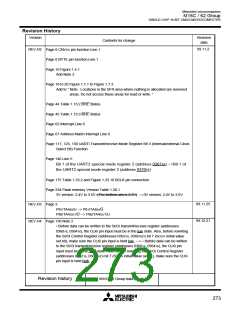
Version
Revision
date
Contents for change
99.11.2
REV.H2
Page 8 CNVSS pin function Line 1
Page 8 BYTE pin function Line 1
Page 10 Figure 1.4.1
Add Note 3
Page 18 to 20 Figure 1.7.1 to Figure 1.7.3
Add to “ Note : Locations in the SFR area where nothing is allocated are reserved
areas. Do not access these areas for read or write. ”
Page 44 Table 1.13.2 _B__H___E__ Status
Page 45 Table 1.13.3 _B__H___E__ Status
Page 62 Interrupt Line 6
Page 67 Address Match Interrupt Line 6
Page 117, 123, 130 UARTi Transmit/receive Mode Register Bit 3 (Internal/external Clock
Select Bit) Function
Page 146 Line 5
Bit 1 of the UART2 special mode register 2 (address 036716) -->Bit 1 of
the UART2 special mode register 2 (address 037616)
Page 175 Table 1.23.2 and Figure 1.23.10 BCLK pin connection
Page 234 Flash memory Version Table 1.28.1
3V version: 2.4V to 3.6V (The bottom aim is 2.2V) -->3V version: 2.4V to 3.6V
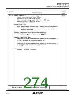
99.11.25
99.12.21
REV.H3
REV.H4
Page 3
__
P81/TA4IN/U --> P81/TA4IN/U
__
P80/TA4OUT/U --> P80/TA4OUT/U
Page 150 Note 2
• Before data can be written to the SI/Oi transmit/receive register (addresses
036016, 036416), the CLKi pin input must be in the low state. Also, before rewriting
the SI/Oi Control Register (addresses 036216, 036616)’s bit 7 (SOUTi initial value
set bit), make sure the CLKi pin input is held low. ---> • Before data can be written
to the SI/Oi transmit/receive register (addresses 036016, 036416), the CLKi pin
input must be in the high state. Also, before rewriting the SI/Oi Control Register
(addresses 036216, 036616)’s bit 7 (SOUTi initial value set bit), make sure the CLKi
pin input is held high.
Revision history
M16C/62 Group data sheet
273

 MITSUBISHI [ Mitsubishi Group ]