Mitsubishi microcomputers
M16C / 62 Group
SINGLE-CHIP 16-BIT CMOS MICROCOMPUTER
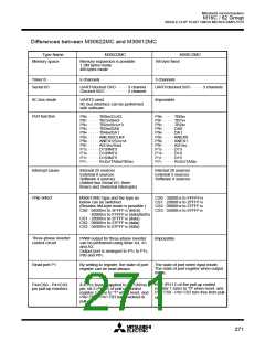
Differences between M30622MC and M30612MC
Type Name
M30622MC
M30612MC
Memory space
Memory expansion is possible
1.2M bytes mode
1M byte fixed
4M bytes mode
Timer B
6 channels
3 channels
UART/clocked SI/O · · · · · 3 channel
Clocked SI/O · · · · · · · · · · 2 channel
Serial I/O
UART/clocked SI/O · · · · · 3 channels
IIC bus mode
Port function
UART2 used
IIC bus interface can be performed
with software
Impossible
P9
P9
P9
P9
P9
P9
P9
P9
P1
P1
P1
P7
0
1
2
3
4
5
6
7
5
6
7
1
· · · · · TB0IN/CLK3
· · · · · TB1IN/SIN
· · · · · TB2IN/SOUT
· · · · · TB3IN/DA0
· · · · · TB4IN/DA1
· · · · · ANEX0/CLK4
· · · · · ANEX1/SOUT
· · · · · ADTRG/SIN
· · · · · D13/INT3
· · · · · D14/INT4
· · · · · D15/INT5
P9
P9
P9
P9
P9
P9
P9
P9
P1
P1
P1
P7
0
1
2
3
4
5
6
7
5
6
7
1
· · · · · TB0IN
· · · · · TB1IN
· · · · · TB2IN
· · · · · DA0
3
3
· · · · · DA1
· · · · · ANEX0
· · · · · ANEX1
· · · · · ADTRG
· · · · · D13
· · · · · D14
· · · · · D15
4
4
· · · · · R
X
D
2
/TA0IN/TB5IN
· · · · · RXD2/TA0IN
Interrupt cause
Chip select
Internal 25 sources
External 8 sources
Software 4 sources
(Added two Serial I/O, three
timers and 3external interrupts)
Internal 20 sources
External 5 sources
Software 4 sources
M30612MC type and the type as
below can be switched
CS0 : 3000016 to FFFFF16
CS1 : 2800016 to 2FFFF16
CS2 : 0800016 to 27FFF16
CS3 : 0400016 to 07FFF16
(Besides 4M-byte mode is possible.)
CS0 : 0400016 to 3FFFF16 (fetch)
4000016 to FFFFF16 (data/facth)
CS1 : 2800016 to 2FFFF16 (data)
CS2 : 0800016 to 27FFF16 (data)
CS3 : 0400016 to 07FFF16 (data)
Three-phase inverter
control circuit
PWM output for three-phase inverter
can be performed using timer A4, A1
and A2.
Impossible
Output port is arranged to P7
P8 and P8
2 to P75,
0
1.
Read port P1
The state of port when input mode.
The state of port register when output
mode.
By setting to register, the state of port
register can be read always.
Bit 2 (PU11) of the pull-up control
register 1 turns to "0" when reset, and
P4
4
/CS0 - P4
7
/CS3
If a Vcc level is applied to the CNVss
pin, bit 2 (PU11) of pull-up control
register 1 turns to "1" when reset, and
pin pull-up resistors
P4
4/
CS0 - P4
7/
CS3 turn free from pull-
P44/ CS0 - P47/ CS3 turn involved in
up.
pull-up.
271

 MITSUBISHI [ Mitsubishi Group ]