Mitsubishi microcomputers
M16C / 61 Group
SINGLE-CHIP 16-BIT CMOS MICROCOMPUTER
Serial I/O
Serial I/O
Serial I/O is configured as three channels: UART0, UART1 and UART2. UART0, UART1 and UART2 each
have an exclusive timer to generate a transfer clock, so they operate independently of each other.
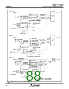
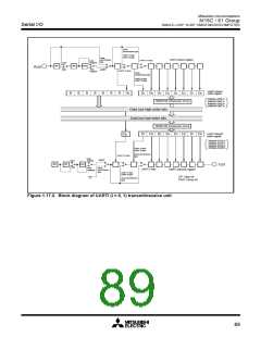
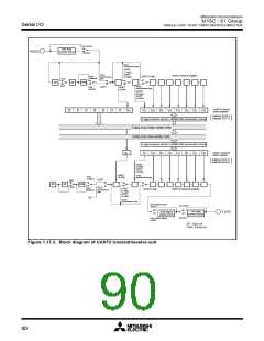
Figure 1.17.1 shows the block diagram of UART0, UART1 and UART2. Figure 1.17.2 and figure 1.17.3
show the block diagram of the transmit/receive unit.
UARTi (i = 0 to 2) has two operation modes: a clock synchronous serial I/O mode and a clock asynchronous
serial I/O mode (UART mode). The contents of the serial I/O mode select bits (bits 0 to 2 at addresses
03A016, 03A816 and 037816) determine whether UARTi is used as a clock synchronous serial I/O or as a
UART.
UART0 through UART2 are almost equal in their functions with minor exceptions. UART2, in particular, is
compliant with the SIM interface with some extra settings added in clock-asynchronous serial I/O mode
(Note). It also has the bus collision detection function that generates an interrupt request if the TXD pin and
the RXD pin are different in level.
Note: SIM : Subscriber Identity Module
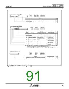
Table 1.17.1 shows the comparison of functions of UART0 through UART2, and Figures 1.17.4 through
1.17.8 show the registers related to UARTi.
Table 1.17.1. Comparison of functions of UART0 through UART2
Function
UART0
UART1
UART2
Possible
CLK polarity selection
Possible
Possible
(Note 1) Possible (Note 1)
(Note 1) Possible (Note 1)
(Note 1) Possible (Note 1)
Possible (Note 1)
(Note 1)
(Note 2)
(Note 1)
LSB first / MSB first selection
Possible
Continuous receive mode selection
Possible
Possible
Transfer clock output from multiple
pins selection
Impossible
Possible
Impossible
Impossible
Possible
Separate CTS/RTS pins
Serial data logic switch
Sleep mode selection
Impossible
Impossible
Possible
Impossible
(Note 4)
(Note 3) Possible (Note 3)
Impossible
Impossible
Possible
TxD, RxD I/O polarity switch
TxD, RxD port output format
Parity error signal output
Bus collision detection
Impossible
N-channel open-drain
output
CMOS output
Impossible
Impossible
CMOS output
Impossible
Impossible
Possible
Possible
(Note 4)
Note 1: Only when clock synchronous serial I/O mode.
Note 2: Only when clock synchronous serial I/O mode and 8-bit UART mode.
Note 3: Only when UART mode.
Note 4: Using for SIM interface.
87

 MITSUBISHI [ Mitsubishi Group ]