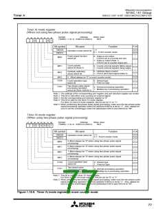
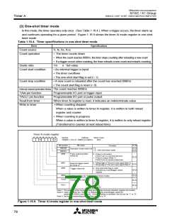
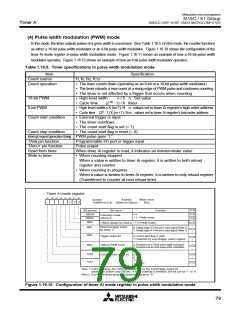
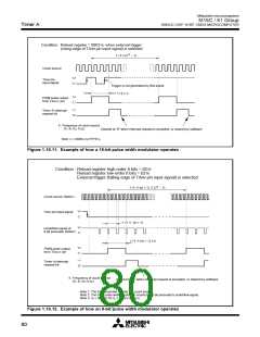
Mitsubishi microcomputers
M16C / 61 Group
SINGLE-CHIP 16-BIT CMOS MICROCOMPUTER
Timer B
Timer B
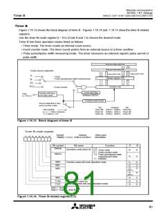
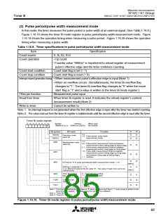
Figure 1.16.13 shows the block diagram of timer B. Figures 1.16.14 and 1.16.15 show the timer B-related
registers.
Use the timer Bi mode register (i = 0 to 2) bits 0 and 1 to choose the desired mode.
Timer B has three operation modes listed as follows:
• Timer mode: The timer counts an internal count source.
• Event counter mode: The timer counts pulses from an external source or a timer overflow.
• Pulse period/pulse width measuring mode: The timer measures an external signal's pulse period or
pulse width.
Data bus high-order bits
Data bus low-order bits
Clock source selection
High-order 8 bits
Low-order 8 bits
f
1
• Timer
Reload register (16)
• Pulse period/pulse width measurement
f
f
8
32
fC32
Counter (16)
• Event counter
Count start flag
Polarity switching
and edge pulse
TBiIN
(i = 0 to 2)
(address 038016
)
Counter reset circuit
Can be selected in only
event counter mode
TBi
Address
TBj
TBj overflow
(j = i – 1. Note, however,
j = 2 when i = 0)
Timer B0 039116 039016 Timer B2
Timer B1 039316 039216 Timer B0
Timer B2 039516 039416 Timer B1
Figure 1.16.13. Block diagram of timer B
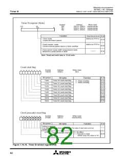
Timer Bi mode register
Symbol
Address
When reset
00XX00002
b7 b6 b5 b4 b3 b2 b1 b0
TBiMR(i = 0 to 2) 039B16 to 039D16
R
W
Bit symbol
Function
Bit name
b1 b0
TMOD0
Operation mode select bit
0 0 : Timer mode
0 1 : Event counter mode
1 0 : Pulse period/pulse width
measurement mode
1 1 : Inhibited
TMOD1
MR0
MR1
MR2
Function varies with each operation mode
(Note 1)
(Note 2)
MR3
TCK0
TCK1
Count source select bit
(Function varies with each operation mode)
Note 1: Timer B0.
Note 2: Timer B1, timer B2.
Figure 1.16.14. Timer B-related registers (1)
81

 MITSUBISHI [ Mitsubishi Group ]