Mitsubishi microcomputers
M16C / 61 Group
SINGLE-CHIP 16-BIT CMOS MICROCOMPUTER
Timer A
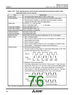
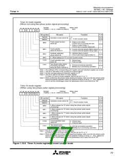
Timer Ai mode register
(When not using two-phase pulse signal processing)
Symbol
Address
When reset
0016
b7 b6 b5 b4 b3 b2 b1 b0
TAiMR(i = 2 to 4) 039816 to 039A16
0
0 1
R W
Bit symbol
Bit name
Function
b1 b0
TMOD0
TMOD1
Operation mode select bit
0 1 : Event counter mode
Pulse output function
select bit
0 : Pulse is not output
MR0
(TAiOUT pin is a normal port pin)
1 : Pulse is output (Note 1)
(TAiOUT pin is a pulse output pin)
Count polarity
select bit (Note 2)
0 : Counts external signal's falling edges
1 : Counts external signal's rising edges
MR1
MR2
0 : Up/down flag's content
1 : TAiOUT pin's input signal (Note 3)
Up/down switching
cause select bit
0 : (Must always be “0” in event counter mode)
MR3
TCK0
0 : Reload type
1 : Free-run type
Count operation type
select bit
Two-phase pulse signal
processing operation
select bit (Note 4)(Note 5)
TCK1
0 : Normal processing operation
1 : Multiply-by-4 processing operation
Note 1: The settings of the corresponding port register and port direction register are invalid.
Note 2: This bit is valid when only counting an external signal.
Note 3: Set the corresponding port direction register to “0”.
Note 4: This bit is valid for the timer A3 mode register.
For timer A2 and A4 mode registers, this bit can be “0 ”or “1”.
Note 5: When performing two-phase pulse signal processing, make sure the two-phase pulse
signal processing operation select bit (address 038416) is set to “1”. Also, always be
sure to set the event/trigger select bit (addresses 038216 and 038316) to “00”.
Timer Ai mode register
(When using two-phase pulse signal processing)
Symbol
Address
When reset
0016
b7 b6 b5 b4 b3 b2 b1 b0
TAiMR(i = 2 to 4) 039816 to 039A16
0
1 0 0 0 1
Bit symbol
Bit name
Function
R W
b1 b0
TMOD0
TMOD1
Operation mode select bit
0 1 : Event counter mode
0 (Must always be “0” when using two-phase pulse signal
processing)
MR0
MR1
MR2
0 (Must always be “0” when using two-phase pulse signal
processing)
1 (Must always be “1” when using two-phase pulse signal
processing)
0 (Must always be “0” when using two-phase pulse signal
processing)
MR3
Count operation type
select bit
0 : Reload type
1 : Free-run type
TCK0
Two-phase pulse
processing operation
select bit (Note 1)(Note 2)
TCK1
0 : Normal processing operation
1 : Multiply-by-4 processing operation
Note 1: This bit is valid for timer A3 mode register.
For timer A2 and A4 mode registers, this bit can be “0” or “1”.
Note 2: When performing two-phase pulse signal processing, make sure the two-phase pulse
signal processing operation select bit (address 038416) is set to “1”. Also, always be
sure to set the event/trigger select bit (addresses 038216 and 038316) to “00”.
Figure 1.16.8. Timer Ai mode register in event counter mode
77

 MITSUBISHI [ Mitsubishi Group ]