MT93L16
Preliminary Information
Address:
16h Read
Receive (Rin) Peak Detect Register 1 (RIPD1)
7
6
5
4
3
2
1
0
Power Up
Reset 00h
RIPD
RIPD
RIPD
3
RIPD
RIPD
RIPD
0
RIPD
5
RIPD
1
4
6
2
7
MSB
LSB
RIPD
RIPD
RIPD
RIPD
RIPD
RIPD
RIPD
RIPD
0
1
2
3
4
5
6
7
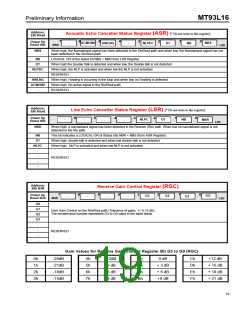
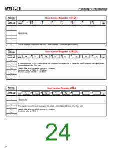
These peak detector registers allow the user to monitor the receive in signal (Rin) peak level at reference point R1 (see
Figure #1). The information is in 16-bit 2’s complement linear coded format presented in two 8 bit registers. The high byte
is in Register 2 and the low byte is in Register 1.
Address:
17h Read
Receive (Rin) Peak Detect Register 2 (RIPD2)
Power Up
Reset 00h
7
6
5
4
3
2
1
0
RIPD
RIPD
RIPD
11
RIPD
RIPD
RIPD
8
RIPD
13
RIPD
9
12
14
10
15
MSB
LSB
7
RIPD
RIPD
8
MSB
9
RIPD
RIPD
RIPD
RIPD
RIPD
RIPD
10
11
12
13
14
15
See Above Description
Address:
18h Read
Receive (Rin) ERROR Peak Detect Register 1 (REPD1)
7
6
5
4
3
2
1
0
REPD
Power Up
Reset 00h
REPD
REPD
REPD
2
REPD
REPD
REPD
REPD
1
4
3
6
5
0
7
MSB
LSB
REPD
REPD
REPD
REPD
REPD
REPD
REPD
REPD
0
1
2
3
4
5
6
7
These peak detector registers allow the user to monitor the error signal peak level at reference point R2 (see Figure #1).
The information is in 16-bit 2’s complement linear coded format presented in two 8 bit registers. The high byte is in Register
2 and the low byte is in Register 1.
Address:
19h Read
Receive (Rin) ERROR Peak Detect Register 2 (REPD2)
7
6
5
4
3
2
1
0
Power Up
Reset 00h
REPD
REPD
8
REPD
REPD
REPD
REPD
REPD
10
REPD
9
12
15
14
13
11
MSB
LSB
REPD8
REPD9
See above description
REPD10
REPD11
REPD12
REPD13
REPD14
REPD15
20

 MITEL [ MITEL NETWORKS CORPORATION ]