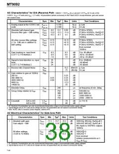
MT9092
AC Electrical Characteristics† - Microport Timing (see Figure 13)
‡
Characteristics
Receive data setup
Sym
Min
Typ
Max
Units
Test Conditions
1
2
3
A
B
C
10
10
ns
ns
ns
Receive data hold
Transmit data delay from clock
falling edge
80
80
80
0
50 pF
4
5
6
7
8
High Z to valid data from SCLK
falling edge
D
E
F
ns
ns
ns
ns
ns
50 pF
50 pF
Valid data to high Z from CS rising
edge
Current transmit data hold
from clock falling edge
Chip Select to SCLK setup and
hold times
G
H
0
SCLK clock period (3 MHz)
333
† Timing is over recommended temperature range & recommended power supply voltages.
‡ Typical figures are at 25°C and are for design aid only: not guaranteed and not subject to production testing.
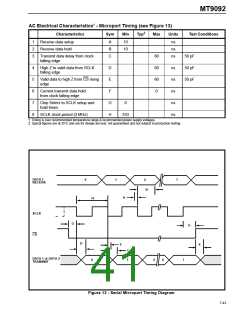
DATA 1
RECEIVE
0
1
2
7
B
A
H
SCLK
CS
G
G
D
E
F
C
DATA 1 or DATA 2
TRANSMIT
0
1
2
6
7
Figure 13 - Serial Microport Timing Diagram
7-43

 MITEL [ MITEL NETWORKS CORPORATION ]