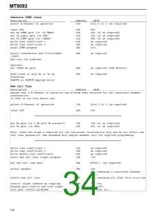
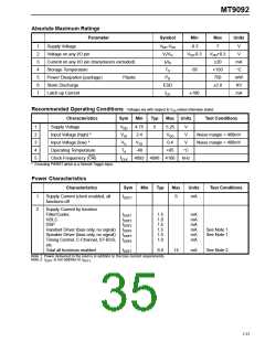
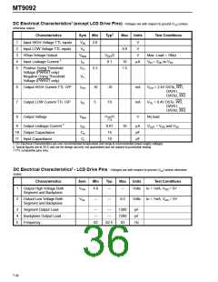
MT9092
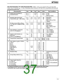
AC Characteristics† for D/A (Receive) Path - 0dBm0 = 1.421Vrms for µ-Law and 1.477Vrms for A-Law, at the
CODEC. (VRef = 0.5volts and VBias = 2.5 volts). All parameters pertain exclusively to the Filter/CODEC except absolute gain and receive
idle channel noise.
‡
Characteristics
Sym
Min
Typ
Max
Units
Test Conditions
µ-Law
1 Analog output at the CODEC full ALo3.17
5.704
5.906
Vp-p
Vp-p
scale
ALo3.14
A-Law
2 Absolute half-channel gain.
Receive filter gain = 0dB setting
GAR1
GAR2
GAR3
-0.6
-12.9 -12.3
-10.3
0.2
0.95
-11.8
-9.1
dB
dB
dB
PCM to SPKR±
PCM to HSPKR±, RxA/u=0*
PCM to HSPKR±, RxA/u=1*
1020Hz
-9.7
All other receive filter settings
(-1 to -7dB) are in addition to
0dB setting
GAR1
GAR2
GAR3
-0.15
-0.15
-0.15
+0.15
+0.15
+0.15
dB
dB
dB
PCM to SPKR±
PCM to HSPKR±, RxA/u=0*
PCM to HSPKR±, RxA/u=1*
from nominal
1020Hz
3 Gain tracking vs. input level
CCITT G.714 Method 2
GTR
-0.3
-0.6
-1.6
0.3
0.6
1.6
dB
dB
dB
3 to -40 dBm0
-40 to -50 dBm0
-50 to -55 dBm0
4 Signal to total distortion vs. input
level.
GQR
35
29
24
dB
dB
dB
0 to -30dBm0
-40 dBm0
-45 dBm0
CCITT G.714 Method 2
5 Receive Idle Channel Noise
NCR
NPR
15.5 dBrnC0 µ-Law
-75
dBrn0p A-Law
6 Gain relative to gain at 1020Hz
200 Hz
GRR
0.25
0.25
0.25
-12.5
-25
dB
dB
dB
dB
dB
300-3000 Hz
3000-3400 Hz
4000 Hz
-0.25
-0.90
>4600 Hz
7 Absolute Delay
DAR
DDR
240
µs
at frequency of min. delay
8 Group Delay relative to D
750
380
130
750
µs
µs
µs
µs
500-600 Hz
AR
600-1000 Hz
1000-2600 Hz
2600 - 2800 Hz
9 Crosstalk
D/A to A/D
A/D to D/A
CTRT
CTTR
-74
-80
dB
dB
G.714.16
† AC Electrical Characteristics are over recommended temperature range & recommended power supply voltages.
‡ Typical figures are at 25°C and are for design aid only: not guaranteed and not subject to production testing.
* Note: RxA/u, refer to General Control Register, address 0Fh.
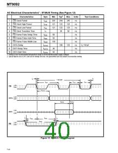
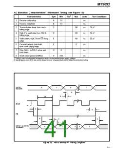
AC Electrical Characteristics† for Side-tone Path
‡
Characteristics
Sym
Min
Typ
Max
Units
Test Conditions
1
Absolute path gain
Gain adjust = 0dB
GAS1
GAS2
-17.2 -16.7 -16.2
-13.1 -12.6 -12.1
dB
dB
SIDEA/u, MICA/u, RxA/u all 0
SIDEA/u, MICA/u, RxA/u all 1
M± inputs to HSPKR± outputs
1000Hz
All other settings
(-9.96 to +9.96dB)
GAS
GAS
-0.3
-0.3
+0.3
+0.3
dB
dB
SIDEA/u=0
SIDEA/u=1
from nominal
relative measurements w.r.t.
G
AS1 & GAS2
† AC Electrical Characteristics are over recommended temperature range & recommended power supply voltages.
‡ Typical figures are at 25°C and are for design aid only: not guaranteed and not subject to production testing.
7-40

 MITEL [ MITEL NETWORKS CORPORATION ]