MT9092
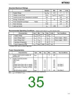
Absolute Maximum Ratings
Parameter
Symbol
Min
Max
Units
1
2
3
4
5
6
7
Supply Voltage
VDD-VSS
VI/VO
II/IO
-0.3
7
VDD+0.3
±20
V
V
Voltage on any I/O pin
VSS-0.3
Current on any I/O pin (transducers excluded)
Storage Temperature
mA
°C
TS
-65
+150
750
Power Dissipation (package)
Static Discharge
Plastic
PD
mW
KV
mA
ESD
ILU
±2.0
Latch-up Current
±100
Recommended Operating Conditions - Voltages are with respect to VSS unless otherwise stated.
Characteristics
Supply Voltage
Sym
Min
Typ
Max Units
Test Conditions
1
2
3
4
5
VDD
VIH
VIL
4.75
2.4
5
5.25
VDD
0.4
V
V
Input Voltage (high) *
Input Voltage (low) *
Operating Temperature
Clock Frequenecy (C4i)
Noise margin = 400mV
Noise margin = 400mV
VSS
-40
V
TA
+85
°C
kHz
fCLK
4092 4096 4100
* Excluding PWRST which is a Schmitt Trigger Input.
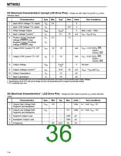
Power Characteristics
Characteristics
Sym
Min
Typ
Max
Units
Test Conditions
1
2
Supply Current (clock enabled, all
functions off
IDDC1
6
mA
Supply Current by function
Filter/Codec
HDLC
DSP
Handset Driver (bias only, no signal)
Speaker Driver (bias only, no signal)
Timing Control, C-Channel, ST-BUS, IDDF6
etc.
IDDF1
IDDF2
IDDF3
IDDF4
IDDF5
1.5
1.0
1.5
1.5
1.5
1.0
mA
mA
mA
mA
mA
mA
See Note 1.
See Note 1.
Total all functions enabled
IDDFT
8.0
14
mA
See Note 2.
Note 1: Power delivered to the load is in addition to the bias current requirements.
Note 2: IDDFT is not additive to IDDC1
.
7-37

 MITEL [ MITEL NETWORKS CORPORATION ]