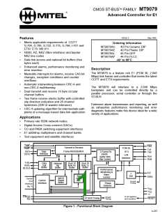
MT9079
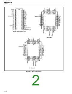
Pin Description
Pin #
Name
Description (see notes 1, 2 and 3)
DIP PLCC QFP
1
1
39 RESET RESET (Input): Low - maintains the device in a reset condition. High - normal
operation. The MT9079 should be reset after power-up. The time constant for a
power-up reset circuit (see Figure 11) must be a minimum of five times the rise time of
the power supply. In normal operation, the RESET pin must be held low for a minimum
of 100 nsec. to reset the device.
2
3
2
3
40
DSTo Data ST-BUS (Output): A 2.048 Mbit/s serial output stream which contains the 30
PCM or data channels received from the PCM 30 line. See Figure 4b.
41
RxDL Receive Data Link (Output): A 4 kbit/s serial stream which is demultiplexed from a
selected national bit (non-frame alignment signal) of the PCM 30 receive signal.
Received DL data is clocked out on the rising edge of DLCLK, see Figure 20.
4
5
4
5
42
TxDL Transmit Data Link (Input): A 4 kbit/s serial stream which is multiplexed into a
selected national bit (non-frame alignment signal) of the PCM 30 transmit signal.
Transmit DL data is clocked in on the rising edge of internal clock IDCLK, see Figure
21.
43 DLCLK Data Link Clock (Output): A 4 kHz clock signal used to clock out DL data (RxDL) on
its rising edge. It can also be used to clock DL data in and out of external serial
controllers (i.e., MT8952). See TxDL and RxDL pin descriptions.
-
6
7
44
1
NC
No Connection.
6
IRQ
Interrupt Request (Output): Low - interrupt request. High - no interrupt request.
IRQ is an open drain output that should be connected to VDD through a pull-up resistor.
An active CS signal is not required for this pin to function.
7
8
2
D0
[P]
Data 0 (Three-state I/O): The least significant bit of the bidirectional data bus of the
parallel processor interface.
SIO
[S]
Serial Input/Output (Three state I/O): This pin function is used in serial controller
mode and can be configured as control data input/output for Intel operation (connect
to controller pin RxD). Input data is sampled LSB first on the rising edge of SCLK; data
is output LSB first on the falling edge of SCLK. It can also be configured as the control
data output for Motorola and National Microwire operation (data output MSB first on
the falling edge of SCLK). See CS pin description.
CSTo0 Control ST-BUS Zero (Output): A 2.048 Mbit/s serial status stream which provides
[ST] device status, performance monitoring, alarm status and phase status data.
8-14 9-15 3-9 D1-D7 Data 1 to Data 7 (Three-state I/O): These signals, combined with D0, form the
[P]
VDD
NC
bidirectional data bus of the parallel processor interface (D7 is the most significant bit).
Positive Power Supply (Input): +5V ± 10%.
No Connection.
15 16 10
17 11
16 18 12
-
AC4 Address/Control 4 (Input): The most significant address and control input for the
[P] non-multiplexed parallel processor interface.
ST/SC ST-BUS/Serial Controller (Input): High - selects ST-BUS mode of operation.
[ST S] Low - selects serial controller mode of operation.
17- 19- 13- AC3-AC Address/Control
3
to
0
(Inputs): Address and control inputs for the
20 22 16
0
non-multiplexed parallel processor interface. AC0 is the least significant input.
[P]
4-239

 MITEL [ MITEL NETWORKS CORPORATION ]