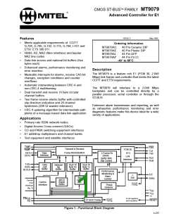
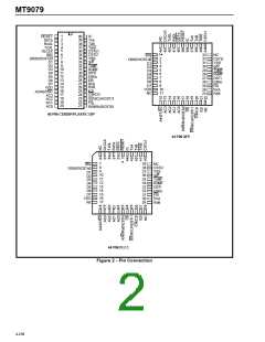
MT9079
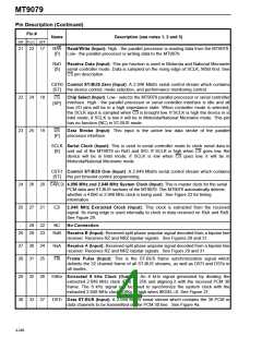
Pin Description (Continued)
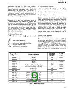
Pin #
Name
Description (see notes 1, 2 and 3)
DIP PLCC QFP
21 23 17
R/W Read/Write (Input): High - the parallel processor is reading data from the MT9079.
[P] Low - the parallel processor is writing data to the MT9079.
RxD Receive Data (Input): This pin function is used in Motorola and National Microwire
[S]
serial controller mode. Data is sampled on the rising edge of SCLK, MSB first. See
CS pin description.
CSTi0 Control ST-BUS Zero (Input): A 2.048 Mbit/s serial control stream which contains
[ST] the device control, mode selection, and performance monitoring control.
22 24 18
CS
Chip Select (Input): Low - selects the MT9079 parallel processor or serial controller
interface. High - the parallel processor or serial controller interface is idle and all
bus I/O pins will be in a high impedance state. When controller mode is selected,
the SCLK input is sampled when CS is brought low. If SCLK is high the device in is
Intel mode; if SCLK is low it will be in Motorola/National Microwire mode. This pin
has no function (NC) in ST-BUS mode.
[SP]
23 25 19
DS
[P]
Data Strobe (Input): This input is the active low data strobe of the parallel
processor interface.
SCLK Serial Clock (Input): This is used in serial controller mode to clock serial data in
[S]
and out of the MT9079 on RxD and SIO. If SCLK is high when CS goes low, the
device will be in Intel mode; if SCLK is low when CS goes low, it will be in
Motorola/National Microwire mode.
CSTi1 Control ST-BUS One (Input): A 2.048 Mbit/s serial control stream which contains
[ST] the per timeslot control programming.
24 26 20 C4i/C2i 4.096 MHz and 2.048 MHz System Clock (Input): This is master clock for the serial
PCM data and ST-BUS sections of the MT9079. The MT9079 automatically detects
whether a 4.096 or 2.048 MHz clock is being used. See Figure 22 for timing
information.
25 27 21
E2i
2.048 MHz Extracted Clock (Input): This clock is extracted from the received
signal. Its rising edge is used internally to clock in data received on RxA and RxB.
See Figure 29.
-
28 22
NC
No Connection.
26 29 23
27 30 24
28 31 25
RxB Receive B (Input): Received split phase unipolar signal decoded from a bipolar line
receiver. Receives RZ and NRZ bipolar signals. See Figures 29 and 31.
RxA Receive A (Input): Received split phase unipolar signal decoded from a bipolar line
receiver. Receives RZ and NRZ bipolar signals. See Figurs 29 and 31.
F0i
Frame Pulse (Input): This is the ST-BUS frame synchronization signal which
delimits the 32 channel frame of all ST-BUS streams, as well as DSTi and DSTo in
all modes.
29 32 26
E8Ko Extracted 8 kHz Clock (Output): An 8 kHz signal generated by dividing the
extracted 2.048 MHz clock (E2i) by 256 and aligning it with the received PCM 30
frame. The 8 kHz signal can be used to synchronize the system clock with the
extracted 2.048 MHz clock. E8Ko is high when 8KSEL=0. See Figure 27.
30 33 27
DSTi Data ST-BUS (Input). A 2.048 Mbit/s serial stream which contains the 30 PCM or
data channels to be transmitted on the PCM 30 line. See Figure 4a.
4-240

 MITEL [ MITEL NETWORKS CORPORATION ]