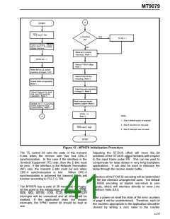
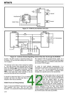
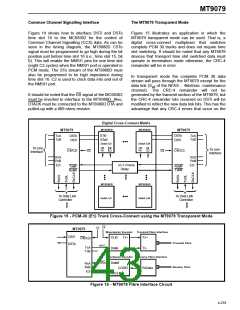
MT9079
Absolute Maximum Ratings* - Voltages are with respect to ground (VSS) unless otherwise stated.
Parameter
Symbol
Min
Max
Units
1
2
3
4
5
6
7
Supply Voltage
VDD
VI
-0.3
-0.3
7
V
Voltage at Digital Inputs
Current at Digital Inputs
Voltage at Digital Outputs
Current at Digital Outputs
Storage Temperature
VDD + 0.3
30
V
mA
V
II
VO
IO
-0.3
-65
VDD + 0.3
30
mA
°C
TST
P
150
Package Power Dissipation
800
mW
* Exceeding these values may cause permanent damage. Functional operation under these conditions is not implied.
Recommended Operating Conditions - Voltages are with respect to ground (VSS) unless otherwise stated.
Characteristics
Sym
Min
Typ
Max
Units
Conditions/Notes
1
2
Operating Temperature
Supply Voltage
TOP
VDD
-40
4.5
85
°C
V
5.5
DC Electrical Characteristics† - Voltages are with respect to ground (V ) unless otherwise stated.
SS
Characteristics
Power Dissipation
Sym Min
Typ
Max
Units
Conditions/Notes
1
2
3
4
5
6
7
8
PD
39
7
mW
mA
V
Outputs unloaded
Outputs unloaded
Supply Current
IDD
Input High Voltage
Input Low Voltage
Current Leakage
Output High Current
Output Low Current
Pin Capacitance
VIH
VIL
ILK
IOH
IOL
CP
2.0
0
VDD
0.8
10
V
µA
mA
mA
pF
0≤V≤VDD See Note 1
Source VOH=2.4 V
Sink VOL=0.4 V
8pF typical
12
15
† Characteristics are over the ranges of recommended operating temperature and supply voltage.
Notes:
1. Maximum leakage on pins (output pin in high impedance state) is over an applied voltage (V).
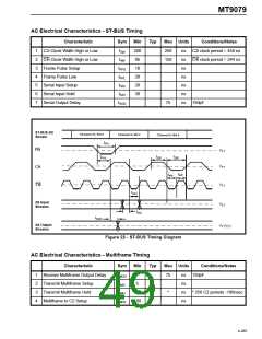
AC Electrical Characteristics - Timing Parameter Measurement Voltage Levels
Characteristics
Sym
Level
Units
Conditions/Notes
1
2
TTL Threshold Voltage
VTT
VCT
1.5
V
V
See Note 1
CMOS Threshold Voltage
0.5VDD
See Note 1
3
Rise/Fall Threshold Voltage High
VHM
2.0
0.7VDD
V
V
TTL
CMOS
See Note 1
See Note 1
4
Rise/Fall Threshold Voltage Low
VLM
0.8
0.3VDD
V
V
TTL
CMOS
Notes:
1. Timing for output signals is based on the worst case result of the combination of TTL and CMOS thresholds.
4-281

 MITEL [ MITEL NETWORKS CORPORATION ]