MT9079
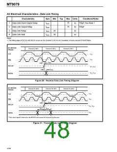
AC Electrical Characteristics - Data Link Timing
Characteristic
Sym
Min
Typ
Max Units
Conditions/Notes
1
2
3
Data Link Clock Output Delay
Data Link Output Delay
Data Link Setup
tDCD
tDOD
tDLS
tDLH
75
75
ns
ns
ns
ns
150pF, See Note 1
150pF
20
30
4
Data Link Hold
Notes:
1. The falling edge of DLCLK and IDCLK occurs on the channel 0, bit 4 to bit 3 boundary of every second ST-BUS frame.
ST-BUS Bit
Stream
Channel 0, Bit 4
Channel 0, Bit 3
Channel 0, Bit 2
C2i
VTT
VTT
C4i
tDCD
DLCLK
VTT, VCT
tDOD
VTT, VCT
RxFDL
Figure 20 - Receive Data Link Timing Diagram
ST-BUS Bit
Stream
Channel 16, Bit 4
Channel 16, Bit 3
Channel 16, Bit 2
VTT
C2i
VTT
C4i
tDCD
IDCLK*
VTT, VCT
tDLS
tDLH
VTT
TxFDL
* This clock signal is internal to the MT9079 and cannot be accessed by the user.
Figure 21 - Transmit Data Link Timing Diagram
4-284

 MITEL [ MITEL NETWORKS CORPORATION ]