Preliminary Information
MT9076
Bit
Name
Functional Description
7-0
TxCNT7-0
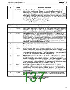
Low Transmit Byte Count Register. This register, along with the Extended
Transmit Byte Count Register indicates the length of the packet about to be
transmitted. For a packet size of 255 or less it is only necessary to write this
register. When this register reaches the count of one, the next write to the Tx FIFO
will be tagged as an end of packet byte. The counter decrements at the end of the
write to the Tx FIFO. If the Cycle bit of Control Register 2 is set high, the counter will
cycle through the programmed value continuously.
Table 168 - Low Transmit Byte Count Register
(Page B,C & D, Address 1AH)
Bit
Name
Functional Description
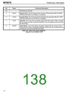
7
HRST
HDLC Reset. When this bit is set to one, the HDLC will be reset. This is similar to
RESET being applied, the only difference being that this bit will not be reset. This bit
can only be reset by writing a zero twice to this location or applying RESET.
6
RTLOOP
RT Loopback. When this bit is high, receive to transmit HDLC loopback will be
activated. Receive data, including end of packet indication, but not including flags or
CRC, will be written to the TX FIFO as well as the RX FIFO. When the transmitter is
enabled, this data will be transmitted as though written by the microprocessor. Both
good and bad packets will be looped back. Receive to transmit loopback may also
be accomplished by reading the RX FIFO using the microprocessor and writing
these bytes, with appropriate tags, into the TX FIFO.
5
4
3
- -
- -
Reserved. Must be set to 0 for normal operation.
Reserved. Must be set to 0 for normal operation.
CRCTST
CRC Remainder Test. This bit allows direct access to the CRC Comparison
Register in the receiver through the serial interface. After testing is enabled, serial
data is clocked in until the data aligns with the internal comparison (16 RXC clock
cycles) and then the clock is stopped. The expected pattern is F0B8 hex. Each bit
of the CRC can be corrupted to allow more efficient testing.
2
FTST
FIFO Test. This bit allows the writing to the RX FIFO and reading of the TX FIFO
through the microprocessor to allow more efficient testing of the FIFO status/
interrupt functionality. This is done by making a TX FIFO write become a RX FIFO
write and a RX FIFO read become a TX FIFO read. In addition, EOP/FA and RQ8/
RQ9 are re-defined to be accessible (i.e. RX write causes EOP/FA to go to RX fifo
input; TX read looks at output of TX fifo through RQ8/RQ9 bits).
1
0
ARTST
HLOOP
Address Recognition Test. This bit allows direct access to the Address
Recognition Registers in the receiver through the serial interface to allow more
efficient testing. After address testing is enabled, serial data is clocked in until the
data aligns with the internal address comparison (16 RXc clock cycles) and then
clock is stopped.
TR Loopback. When high, transmit to receive HDLC loopback will be activated.
The packetized transmit data will be looped back to the receive input. RXEN and
TXEN bits must also be enabled.
Table 169 - HDLC Test Control Register
(Page B,C & D, Address 1BH)
133

 MITEL [ MITEL NETWORKS CORPORATION ]