MT9076
Preliminary Information
Bit
Name
Functional Description
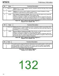
7 - 2
ADR16-11 Address 16 - 11. A six bit address used for comparison with the first byte of the received
address. ADR16 is MSB.
1
0
ADR10
A1EN
Address 10. This bit is used in address comparison if a seven bit address is being
checked for (control bit four of control register 2 is set).
First Address Comparison Enable. When this bit is high, the above six (or seven) bit
address is used in the comparison of the first address byte.
If address recognition is enabled, any packet failing the address comparison will not be
stored in the RX FIFO. A1EN must be high for All-call (1111111) address recognition for
single byte address. When this bit is low, this bit mask is ignored in address comparison
Table 157 - HDLC Address Recognition Register 1
(Page B,C & D, Address 10H)
Bit
Name
Functional Description
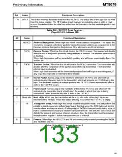
7 - 1
ADR26-20 Address 26 - 20. A seven bit address used for comparison with the second byte of the
received address. ADR26 is MSB. This mask is ignored (as well as first byte mask) if all
call address (1111111) is received.
0
A2EN
Second Address Comparison Enable. When this bit is set high, the above seven bit
address is used in the comparison of the second address byte.
If address recognition is enabled, any packet failing the address comparison will not be
stored in the RX FIFO. A2EN must be high for All-call address recognition. When this bit is
low, this bit mask is ignored in address comparison
Table 158 - HDLC Address Recognition Register 2
(Page B,C & D, Address 11H)
Bit
Name
Functional Description
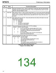
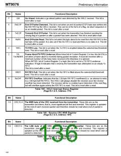
7 - 0
BIT7-0 This eight bit word is tagged with the two status bits from the control register 1 (EOP and FA),
and the resulting 10 bit word is written to the TX FIFO. The FIFO status is not changed
immediately after a write or read occurs. It is updated after the data has settled and the
transfer to the last available position has finished.
Table 159 - TX FIFO Write Register
(Page B,C & D, Address 12H)
128

 MITEL [ MITEL NETWORKS CORPORATION ]