Preliminary Information
MT9075A
Function
Status
PCM 30 Channel Zero
CRC
Frame/
Type
CRC
Mode
Loopbacks
Termination
Deactivated
1
C1
0
2
0
1
0
1
0
1
0
1
0
1
0
1
0
1
0
1
3
0
4
5
6
7
8
0/FAS
1
1
0
1
1
Transmit FAS
C 0011011
n
Transmit non-FAS
Transmit MFAS (CAS)
Data Link
1/S 1111111
1/NFAS
2/FAS
A
0
Sa4 Sa5 Sa6 Sa7 Sa8
n
00001111
Deactivated
Activated
C2
0
1
1
0
1
1
3/NFAS
4/FAS
A
0
Sa4 Sa5 Sa6 Sa7 Sa8
CRC Interworking
Signalling
C3
1
1
1
0
1
1
CAS Registers
Deactivated
5/NFAS
6/FAS
A
0
Sa4 Sa5 Sa6 Sa7 Sa8
ABCD Bit Debounce
Interrupts
Interrupt Mask Word
Zero unmasked, all
others masked;
C4
0
1
1
0
1
1
7/NFAS
8/FAS
A
0
Sa4 Sa5 Sa6 Sa7 Sa8
interrupts not suspended
C1
1
1
1
0
1
1
RxMF Output
Error Insertion
HDLCs
Signalling Multiframe
Deactivated
9/NFAS
10/FAS
11/NFAS
12/FAS
A
0
Sa4 Sa5 Sa6 Sa7 Sa8
C2
1
1
1
0
1
1
Deactivated
A
0
Sa4 Sa5 Sa6 Sa7 Sa8
Counters
Cleared
C3
1
1
0
1
1
Tx Message Buffer
All locations set to 54H
All locations cleared
Per Time Slot Control
Buffer
13/NFAS E1
14/FAS C4
15/NFAS E2
A
0
Sa4 Sa5 Sa6 Sa7 Sa8
1
1
0
1
1
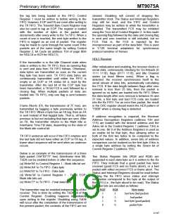
Table 6 - Reset Status
A
Sa4 Sa5 Sa6 Sa7 Sa8
Transmit AIS Operation
Table 7 - FAS and NFAS Structure
indicates position of CRC-4 multiframe alignment signa
The pin TAIS (Transmit AIS, pin 60 in PLCC, pin 48 in
MQFP) allows an all ones signal to be transmitted
from the point of power-up without the need to write
any control registers. During this time the IRQ pin is
tristated. After the interface has been initialized
normal operation can take place by making TAIS
high.
Table 8 illustrates the organization of the MT9075A
transmit and receive national bit buffers. Each row is
an addressable byte of the MT9075A national bit
buffer, and each column contains the national bits of
an odd numbered frame of each CRC-4 Multiframe.
The transmit and receive national bit buffers are
located at page 0DH and 0EH respectively.
National Bit Buffers
Table 7 shows the contents of the transmit and
receive Frame Alignment Signals (FAS) and Non-
frame Alignment Signals (NFAS) of time slot zero of
a PCM 30 signal. Even numbered frames (CRC
Frame # 0, 2, 4,...) are FASs and odd numbered
frames (CRC Frame # 1, 3, 5,...) are NFASs. The bits
of each channel are numbered 1 to 8, with bit 1 being
the most significant and bit 8 the least significant.
Frames 1, 3, 5, 7, 9, 11, 13 & 15 of a CRC-4
Addre
Multiframe
ssable
Bytes
F1 F3 F5 F7 F9 F11 F13 F15
NBB0 Sa4 Sa4 Sa4 Sa4 Sa4 Sa4 Sa4 Sa4
NBB1 Sa5 Sa5 Sa5 Sa5 Sa5 Sa5 Sa5 Sa5
NBB2 Sa6 Sa6 Sa6 Sa6 Sa6 Sa6 Sa6 Sa6
NBB3 Sa7 Sa7 Sa7 Sa7 Sa7 Sa7 Sa7 Sa7
NBB4 Sa8 Sa8 Sa8 Sa8 Sa8 Sa8 Sa8 Sa8
Table 8 - MT9075A National Bit Buffers
Note that the Data Link (DL) pin functions, if
selected, override the transmit national bit buffer
function.
4-143

 MITEL [ MITEL NETWORKS CORPORATION ]