MT9075A
Preliminary Information
of memory is selected, it is only necessary to write to
the CAR when a different page is to be accessed.
See Figures 11 and 12 for timing requirements.
Identification Code
The MT9075A shall be identified by the code
10101010, read from the identification code status
register (page 03H, address 1FH).
Please note that for microprocessors with read/write
cycles less than 200 ns, a wait state or a dummy
operation (for
successive read/write operations to the HDLC FIFO
is required.
C
programming) between two
Reset Operation (Initialization)
The MT9075A can be reset using the hardware
RESET pin (pin 11 in PLCC, pin 84 in MQFP, see pin
description for external reset circuit requirements) or
the software reset bit RST (page 01H, address 11H).
When the device emerges from its reset state it will
begin to function with the default settings described
in Table 6. A reset operation takes 1 full frame (125
us) to complete.
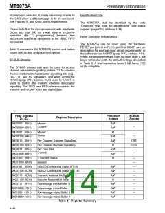
Table 5 associates the MT9075A control and status
pages with access and page descriptions.
ST-BUS Streams
The ST-BUS stream can also be used to access
channel associated signalling nibbles. CSTo contains
the received channel associated signalling bits (e.g.,
ITU-T R1 and R2 signalling), and when control bit
RPSIG (page 01H, address 1AH) is set to 0, CSTi is
used to control the transmit channel associated
signalling. The DSTi and DSTo streams contain the
transmit and receive voice and digital data.
Page Address
Processor
Access
ST-BUS
Access
Register Description
D7 - D0
00000001 (01H)
00000010 (02H)
00000011 (03H)
00000100 (04H)
00000101 (05H)
00000110 (06H)
00000111 (07H)
00001000 (08H)
00001001 (09H)
00001010 (0AH)
00001011 (0BH)
00001100 (0CH)
00001101 (0DH)
00001110 (0EH)
00001111 (0FH)
00010000 (10H)
00010001 (11H)
00010010 (12H)
Master
Control
R/W
R/W
R
--
Master
Status
---
R/W
R/W
R
Per Channel Transmit Signalling
Per Channel Receive Signalling
CSTi
CSTo
Per Time Slot
Control
R/W
R/W
R
---
1 Second Status
---
---
---
---
---
---
---
---
---
---
unused
HDLC0 Control and Status (TS 0)
HDLC1 Control and Status (TS 16)
Transmit National Bit Buffer
Receive National Bit Buffer
Tx message mode Buffer 0
Tx message mode Buffer 1
Rx message mode Buffer 0
Rx message mode Buffer 1
R/W
R/W
R/W
R
R/W
R/W
R/W
R/W
Table 5 - Register Summary
4-142

 MITEL [ MITEL NETWORKS CORPORATION ]