ISO-CMOS MT8976
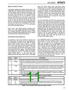
Bipolar Violation Counter
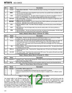
when the phase status word increments above
channel 31, bit 7 or decrements below channel 0, bit
0. The E8Ko signal has a specific relationship with
received DS1 frame. The rising edge of E8Ko occurs
during bit 2, channel 17 of the received DS1 frame.
The Phase Status Word in conjunction with the frame
count bit, can be used to monitor the phase
relationship between the received DS1 frame and
the local ST-BUS frame.
The Bipolar Violation bit in Master Status Word 1 will
toggle after 256 violations have been detected in the
received signal. It has a maximum refresh time of 96
ms. This means that the bit can not change state
faster than once every 96 ms. For example, if there
are 256 violations in 80 ms the BPV bit will not
change state until 96 ms. Any more errors in that
extra 16 ms are not counted. If there are 256 errors
in 200 ms then the BPV bit will change state after
200 ms. In practical terms this puts an upper limit on
the error rate that can be calculated from the BPV
The local 2.048 MHz ST-BUS clock must be phase-
locked to the 1.544 MHz clock extracted from the
received data. When the two clocks are not phase-
locked, the input data rate on the DS1 side will differ
from the output data rate on the ST-BUS side. If the
average input data rate is higher than the average
output data rate, the channel count and bit count in
the phase status word will be seen to decrease over
time, indicating that the E8Ko rising edge, and
therefore, the DS1 frame boundary is moving with
respect to the ST-BUS frame pulse. Conversely, a
lower average input data rate will result in an
increase in the phase reading.
-3
information, but this rate (1.7 X 10 ) is well above
any normal operating condition.
Bits 4 and 3 also provide bipolar violations infor-
mation. Bit 4 will change state after 128 violations.
Bit 3 changes state after 64 bipolar violations. These
bits are refreshed independently and are not subject
to the 96ms refresh rate described above.
DS1/ST-BUS Phase Difference
In an application where it is necessary to minimize
jitter transfer from the received clock to the local
system clock, a phase lock loop with a relatively
large time constant can be implemented using
information provided by the phase status word. In
such a system, the local 2.048 MHz clock is derived
from a precision VCO. Frequency corrections are
made on the basis of the average trend observed in
the phase status word. For example, if the channel
count in the phase status word is seen to increase
over time, the feedback applied to the VCO is used
to decrease the system clock frequency until a
reversal in the trend is observed.
An indication of the phase difference between the
ST-BUS and the DS1 frame can be ascertained from
the information provided by the eight bit Phase
Status Word and the Frame Count bit. Channel
three on CSTo contains the Phase Status Word. Bits
7-3 in this word indicate the number of ST-BUS
channels between the ST-BUS frame pulse and the
rising edge of the E8Ko signal. The remaining three
bits provide one bit resolution within the channel
count indicated by bits 7-3. The frame count bit in
Master Status Word 2 is the ninth and most
significant bit of the phase status word. It will toggle
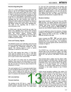
Bit
Name
Description
7-3
2
IC
Internal Connections. Must be kept at 0 for normal operation
Polarity
When set, the applicable channel is not inverted on the transmit or the receive side of the device.
When clear, all the bits within the applicable channel are inverted both on transmit and receive
side.
1
0
Loop
Data
Per Channel Loopback. When set, the received DS0 channel is replaced with the transmitted
DS0 channel. Only one DS0 channel may be looped back in this manner at a time. The transmitted
DS0 channel remains unaffected. When clear the transmit and receive DS0 sections operate
normally.
Data Channel Enable. When set, robbed bit signalling for the applicable channel is disabled.
When clear, every 6th DS1 frame is available for robbed bit signalling. This feature is enabled only
if bit 1 in Master Control Word is low.
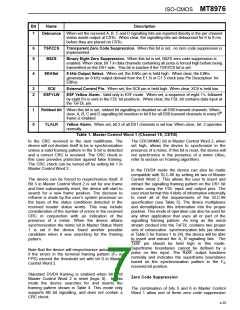
Table 6. Per Channel Control Word 1 Input at CSTi0
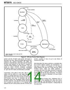
Bit
7-4
Name
Description
Unused
Keep at 0 for normal operation
3
2
1-0
A
B
C, D
These are the 4 signalling bits inserted in the appropriate channels of the DS1 stream being
output from the chip, when in ESF mode. In D3/D4 modes where there are only two signalling
bits, the values of C and D are ignored.
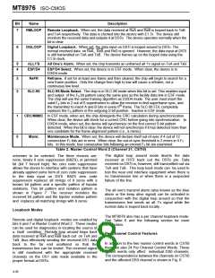
Table 7. Per Channel Control Word 2 Input at CSTi1
4-39

 MITEL [ MITEL NETWORKS CORPORATION ]