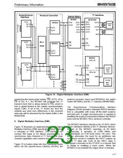
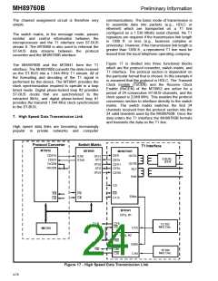
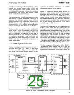
Preliminary Information
MH89760B
.
Absolute Maximum Ratings*
Parameter
Symbol
Min
Max
Units
1
2
3
4
5
6
Supply Voltage with respect to VSS
VDD
-0.3
7
VDD+0.3
15
V
V
Voltage on any pin other than supplies, OUTA or OUTB
Voltage on OUTA or OUTB
V
SS-0.3
V
Current at any pin other than supplies, OUTA or OUTB
Current at OUTA or OUTB
20
mA
mW
°C
200
85
Storage Temperature
TST
-20
* Exceeding these values may cause permanent damage. Functional operation under these conditions is not implied.
Recommended Operating Conditions - Voltages are with respect to ground (VSS) unless otherwise stated.
‡
Parameters
Sym
Min
Typ
Max
Units
Test Conditions
1
2
3
Operating Temperature
Supply Voltage
TOP
VDD
VIH
VIH
VIH
VIL
0
70
5.5
VDD
°C
V
I
4.5
2.4
5.0
3.0
0.3
n
p
u
t
Input High Voltage
V
Digital Inputs
V
Line Inputs
Digital Inputs
Line Inputs
4
Input Low Voltage
VSS
0.4
V
s
V
‡ Typical figures are at 25°C and are for design aid only: not guaranteed and not subject to production testing.
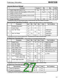
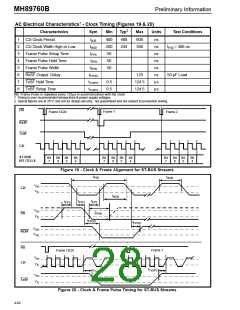
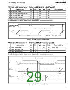
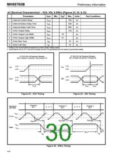
DC Electrical Characteristics - Clocked operation over recommended temperature ranges.
‡
Parameters
Supply Current
Sym
Min
Typ
Max Units
Test Conditions
1
2
3
4
5
6
7
IDD
VIH
VIL
IIL
12
25
mA
V
Outputs Unloaded
Digital Inputs
I
n
p
u
t
Input High Voltage
Input Low Voltage
2.0
0.8
V
Digital Inputs
s
Input Leakage Current
Output High Current
Output Low Current
±1
20
10
±10
µA
mA
mA
Digital Inputs VIN=0 to VDD
Source Current VOH=2.4V
Sink Current VOL=0.4V
IOH
IOL
7
2
O
u
t
p
u
t
Output Low Voltage
OUTA or OUTB
VOL
ZIN
0.25
V
IOL=10mA
8
9
Input Impedance RxT to RxR
RxT or RxR to Gnd
400
1K
Ω
Ω
V
V
s
Schmitt Trigger Input (XSt)
VT+
VT-
4.0
1.5
‡ Typical figures are at 25°C and are for design aid only: not guaranteed and not subject to production testing.
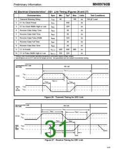
AC Electrical Characteristics† - Capacitance
‡
Characteristics
Sym
Min
Typ
Max
Units
Test Conditions
1
2
Input Pin Capacitance
Output Pin Capacitance
CI
10
10
pF
pF
CO
† Timing is over recommended temperature & power supply voltages.
‡ Typical figures are at 25°C and are for design aid only: not guaranteed and not subject to production testing.
4-81

 MITEL [ MITEL NETWORKS CORPORATION ]