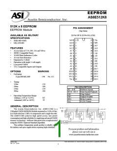
EEPROM
AS8E512K8
Austin Semiconductor, Inc.
ABSOLUTE MAXIMUM RATINGS*
Voltage on Vcc Supply Relative to Vss
*Stresses greater than those listed under "Absolute Maximum
Ratings" may cause permanent damage to the device. This is
a stress rating only and functional operation of the device at
these or any other conditions above those indicated in the
operation section of this specification is not implied. Exposure
to absolute maximum rating conditions for extended periods
may affect reliability.
Supply/Input Voltage Range1.........................-0.6V to +6.25V DC
Voltage on OE\ and A9....................................-0.6V to +13.5V DC
Voltage on all other pins..................................-0.6V to +6.25V DC
Storage Temperature.............................................-65°C to +150°C
Operating Temperature, TA (Ambient)................-55oC to +125oC
Lead Temperature (soldering 10 seconds)........................+300oC
Maximum Junction Temperature**....................................+165°C
NOTE: 1. Including NC pins, with respect to ground.
** Junction temperature depends upon package type, cycle
time, loading, ambient temperature and airflow.
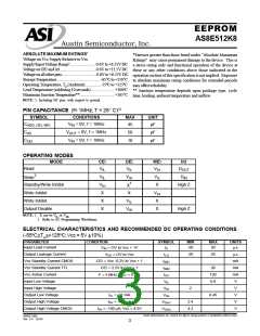
PIN CAPACITANCE (f= 1MHz, T = 25° C)(1)
SYMBOL
CONDITIONS
MAX
UNIT
CADD, OE\, WE\
VIN = 0V, f = 1MHz
45
50
10
pF
CI/O
VOUT = 0V, f = 1MHz
VIN = 0V, f = 1MHz
pF
pF
CCE\
OPERATING MODES
MODE
CE\
OE\
WE\
I/O
Read
VIL
VIL
VIH
VIL
X
DOUT
Write2
VIL
VIH
X
VIH
DIN
X1
X
Standby/Write Inhibit
High Z
Write Inhibit
Write Inhibit
VIH
X
X
VIL
Output Disable
X
X
High Z
VIH
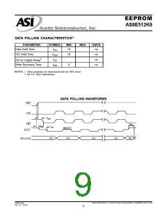
NOTE: 1. X can be VIL or VIH.
2. Refer to AC Programming Waveforms.
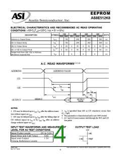
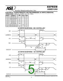
ELECTRICAL CHARACTERISTICS AND RECOMMENDED DC OPERATING CONDITIONS
(-55oC<TA<+125oC;Vcc = 5V +10%)
PARAMETER
CONDITION
SYMBOL
MIN
MAX
UNITS
Input Load Current
-20
20
VIN = OV to Vcc + 1V
ILI
µΑ
Output Leakage Current
Vcc Standby Current CMOS
Vcc Standby Current TTL
Vcc Active Current
-20
20
VI/O = OV to Vcc
CE\ = Vcc -0.2V to Vcc + 1
CE\ = 2.2V to Vcc + 1
F = 5 MHz; IOUT = 0 mA
ILO
ISB1
ISB2
ICC
µΑ
mA
mA
mA
V
20
120
0.8
Input Low Voltage
VIL
Input High Voltage
2
V
VIH
I
OL = 2.1 mA
Output Low Voltage
0.45
V
VOL
VOH1
VOH2
IOH = -400 µA
Output High Voltage
Output High Voltage CMOS
2.4
4.2
V
IOH = -100 µA; Vcc = 4.5V
V
Austin Semiconductor, Inc. reserves the right to change products or specifications without notice.
AS8E512K8
Rev. 2.0 12/99
3

 MICROSS [ MICROSS COMPONENTS ]