TPU 3035, TPU 3040
PRELIMINARY DATA SHEET
P
off
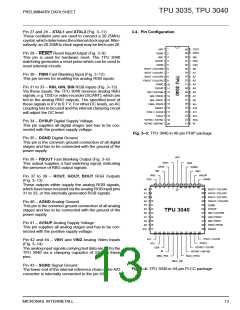
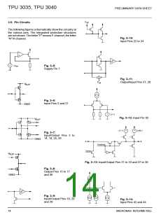
3.5. Pin Circuits
The following figures schematically show the circuitry at
the various pins. The integrated protection structures
arenotshown. Theletter“P”meansP-channel, theletter
“N” N-channel.
Fig. 3–10:
Input Pins 22 to 24
–
+
=
V
Ref
Fig. 3–5:
Supply Pin 1
Fig. 3–11:
Output/Input Pins 27, 28
P
off
V
SUP
P
N
Fig. 3–6:
Input Pins 2 and 21
GND
=
0.7 V
Fig. 3–12: Input Pin 30
V
SUP
P
P
N
=
=
0.7 V
0.46 V
Fig. 3–7:
N
Input/Output Pins 3 to
14, 18, 25, 26
GND
Fastblank
Clamp
V
SUP
P
Fig. 3–13: Input/Output Pins 31 to 33 and 37 to 39
Fig. 3–8:
N
Output Pins 15 to 17
and 36
GND
Fig. 3–9:
Input/Output Pins 19, 20
and 29
Fig. 3–14:
Input Pins 42 and 44
14
MICRONAS INTERMETALL

 MICRONAS [ MICRONAS ]