CCU 3000, CCU 3000-I
CCU 3001, CCU 3001-I
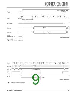
2. Functional Description
2.1. ROM
2.5. PORT 1 to PORT 3, PORT 6 to PORT 8
8 ports belong to the system, of which 5 are 8 bits wide,
one 6 bit, one 4 bit and one 1 bit wide. All port lines of
PORTS 1 to 3 and 6 to 8 can be used as inputs or outputs
independently from each other. One register per port
defines the direction. PORT1 to PORT3 have push-pull
outputs and PORT6 to PORT8 have open drain outputs.
Even a line defined as output can be read, the pin level
being important. This property makes it possible for the
software to find desired and undesired short circuits.
Each port reserves a byte for the direction register and
the data in the I/O page. If the corresponding bit in the
direction register is set to 0, the output mode is switched
on. After a reset, all bits of a direction register are set
to 1. The falling edge of bit 7 of PORT 8 generates inter-
rupts if the priority of the corresponding interrupt control-
ler source (7) is not set to 0.
Thechipisequippedwith32kBytemask-programmable
ROM. The ROM uses up the address space from 8000H
to FFFFH. This ROM can be supplemented or replaced
externally. Only the CCU 3001 has an internal ROM.
2.2. RAM
The RAM area is split into three parts:
– page 0
(address 0 to FFH)
– page 1
(address 100H to 1FFH)
(address 300H to 63FH)
– page 3, 4, 5, 6
2.6. PORT 4
Page 0 offers a particularly fast access to the 65C02 and
is therefore very valuable for fast, compact programs.
Page 1 contains the stack and must therefore also have
RAM. The remaining RAM-memory follows in pages 3,
4, 5, 6, as page 2 is reserved as I/O address space. The
RAM can be kept in the stand-by mode via stand-by pin.
PORT 4 consists of only one line (LSB, P40). After a re-
set, PORT4operatesasaninputonly. AssoonasPORT
4 is written for the first time, it is switched to output mode
(push-pull). Later read accesses read the actual level at
port 4. If bit 3 in the control word is active, P4 is used as
an R/W-line. If the internal CPU is active, R/W is an out-
put line, otherwise it is an input. But P4 has another, very
important function during RESET. The level at P4 during
RESET decides whether the control word is read from
the internal ROM (FFF9H) or from the external memory.
It is therefore important that the desired level during RE-
SET is set at P4. An internal pull-down resistor of ap-
prox. 100kΩ isintegratedintheCCU3001, whichensur-
es that the control word is read by the internal ROM. The
external control word access is obtained via an external
pull-up resistor of approx. 5 kΩ. The CCU 3000 has an
internal pull-up resistor at P4 (external ROM access).
The further mode of operation of the CCU 3000, CCU
3001 depends only on the control word though.
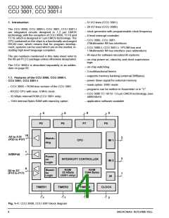
2.3. CPU
The CPU core is fully compatible with the 65C02 micro-
processor. However, not all the pins of the 65C02 proc-
essor are accessible for the user outside the chip. One
switch in the control register allows the CPU to be
switched off, so that an external processor can take over
its tasks. This external processor can of course also be
an in-circuit emulator, which makes near-hardware
emulation possible, even though the status and control
lines of the internal CPU are not accessible. If an exter-
nal processor is used, all hardware blocks of the chip are
as accessible to it as if it were the internal CPU.
Please note that this mode is always necessary for
the CCU 3000 since this device does not have inter-
nal ROM!
2.4. Clock Generator
An integrated two-pin oscillator generates the clock for
the microcontroller. The frequency created by the oscil-
lator can be programmed to be reduced with a divider
by the factor 1 ... 255. This enables the user to decrease
the current consumption by the controller by reducing
the working frequency as well as to increase the access
time for the (slower) external memory. This divider con-
tainsthevalue4afterareset, sothatthesystemcanalso
start with a slow external memory. If the mask-option
OSC is set (EMU version), a switch in the control regis-
ter makes it possible to receive the internal clock Φ2 at
XTAL2. In this case the oscillator must be external and
the clock must be fed to the pin XTAL1. In this way, the
user gets a time reference for internal operations in the
microcomputer. This is especially important with the in-
terrupt controller. The production version of the CCU
does not have this function!
2.7. I/O-Lines P50 to P55
The 6 additional I/O-lines have a two-fold function:
– input or output line (open drain output) or
– fully decoded I/O-select lines (push-pull outputs)
As a rule these lines can be used as input or output lines.
As soon as ports 1 to 4 are used as system bus, they are
lost as I/O-channels. However, a total of 48 port lines (24
inputs and outputs each) can be reconstructed without
difficulties (1 housing for 8 lines), if the additional 6 I/O-
lines of the CCU 3000, CCU 3001 are switched into the
port select mode. They then represent the select lines of
the original ports 1 to 3. Each line can be defined as I/O
or port select line separately. In the I/O-page three bytes
are needed.
MICRONAS INTERMETALL
5

 MICRONAS [ MICRONAS ]