CCU 3000, CCU 3000-I
CCU 3001, CCU 3001-I
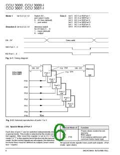
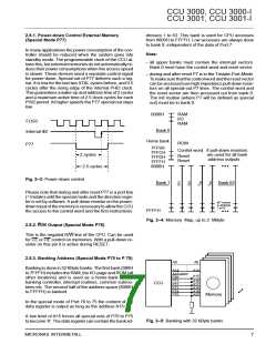
2.8.1. Power-down Control External Memory
(Special Mode P77)
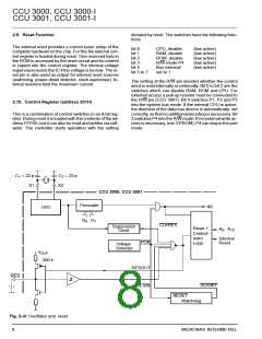
dresses 1 to 63. This bank is used for CPU accesses
from 8000H to FFFFH. Low accesses are always done
to bank 0, independent of the data of Port 7.
In many applications the power consumption of the con-
troller should be reduced when the system goes into
standby mode. The programmable clock of the CCU al-
lows this, but external memories do not automatically re-
duce their power consumptions when the access speed
is slower. These devices need a separate control signal
for power down. Special out of P77 delivers such a sig-
nal. It is low for the last two XTAL cycles before, and 0.5
cycles after the rising edge of the internal PHI2 clock.
This guarantees a wake-up and address time of 2 cycles
and a maximum active time of 2.5 clock cycles for each
PHI2 period. At higher speeds the P77 special out stays
low.
Note:
– all upper banks must contain the interrupt vectors.
Bank 0 must have the control word and reset vector.
– during and after reset P7 is in the Tristate-Port-Mode.
Tomakesurethatthecontrolwordandtheresetvector
can be accessed use high impedance pull-down resis-
tors on all special-out P7 lines. The control word and
the reset vector are then accessed out from bank 0.
The init routine (where P7 will be defined as special
out) must be in bank 0.
0000H
RAM
I/O
FOSC
RAM
Bank 0
Internal Φ2
Home bank
ROM
P77
7FF9H
7FFCH
7FFDH
7FFFH
8000H
Control word if pull-down resistors
2 cycles
are used for all bank
Reset
address outputs
Reset
2.5 cycles
Fig. 2–3: Power-down control
Bank 1
2
3
4
5
Bank 63
Please note that during and after reset P77 is a port line
(= tristate) until the special mode and the direction regis-
ter is set by software. A pull-down resistor on the power-
down input of the memory is necessary to allow the CCU
the access to the control word and the first instructions.
INT vectors
in all Banks
1 to 63
FFFFH
Fig. 2–4: Memory Map, up to 2 MByte
2.8.2. R/W Output (Special Mode P76)
This is the negated R/W-line of the CPU. Can be used
for CE or OE control on memories. With a pull-down re-
sistor on this pin it is active during RESET.
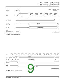
2.8.3. Banking Address (Special Mode P70 to P 75)
A0
A0
Banking is done in 32 KByte banks. The first bank (000H
to 7FFFH) includes the RAM, the I/O-page and ROM (all
other locations) and is used as a home-bank for the
banking controller, interrupt routines, common subrou-
tines etc. The second half of the address space (8000H
to FFFFH) is banked.
A14
A15 open
P70
P71
P72
P73
P74
P75
A14
A15
A16
A17
A18
A19
A20
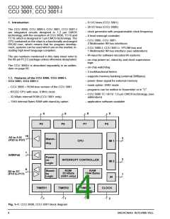
CCU
Memory
In the special mode of Port 70 to 75 the content of the
data register is output as long as the address A15=1.
A low level of A15 forces all special outs of P70 to P75
tobecome‘0’. Thedataregistercancontainthebankad-
Fig. 2–5: Banking with 32 kByte banks
MICRONAS INTERMETALL
7

 MICRONAS [ MICRONAS ]