CCU 3000, CCU 3000-I
CCU 3001, CCU 3001-I
1. Introduction
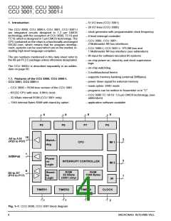
– 51 I/O lines (CCU 3001)
– 26 I/O lines (CCU 3000)
The CCU 3000, CCU 3000-I, CCU 3001, CCU 3001-I
are integrated circuits designed in 1.2 µm CMOS
technology, with the exception of CCU 3000, TC18 and
TC19, which is designed in 1 µmCMOS technology. The
CPU contained on the chips is a functionally unchanged
65C02-core, which means that for program develop-
ment, systems can be used which are on the market; in-
cluding high level language compilers.
– clock generator with programmable clock frequency
– 8 level interrupt controller
– CCU 3000, CCU 3001:
2 Multimaster IM bus interfaces
2
– CCU 3000-I, CCU 3001-I: 1I C/IM bus and
1 Multimaster IM bus interface (see addendum)
– IR-input for software-decoded IR-systems
The pin numbers mentioned in this data sheet refer to
the 68-pin PLCC package unless otherwise designated.
– on-chip power on, stand-by and clock supervision
logic
The CCU 3000-I is described separately in an adden-
dum on page 66.
– on-chip watchdog
– 3 multifunctional timers
– supports memory banking (external 2MBytes)
– power down signal for external memory
– mask option: EMU mode
1.1. Features of the CCU 3000, CCU 3000-I,
CCU 3001, CCU 3001-I
– CCU 3000 = ROM-less version of the CCU 3001
– 65C02 CPU with max. 8 MHz clock
– programs can be written in Assembler or in “C”
– CCU 3000 TC 18/19: 1.0 µm CMOS technology, (see
– 32 kByte internal ROM (CCU 3001 only)
– 1344 internal Bytes RAM with stand-by option
addendum)
– application software available
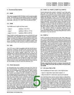
6
8
8
5
P5
P6
P7
P8
16
1
A0 to A15
3
Watch–
dog
(P20 to P37)
CPU
IM 1
R/W/P40
Power
on
Logic
3
1
INTERRUPT CONTROLLER
IM 2
IR
8
ROM
32 kByte
(3001 only)
RAM
1344 Bytes
Stand–
by
Logic
D0 to D7
(P10 to P17)
TIMER1
1
TIMER2
TIMER3
CLOCK
2
1
1
Fig. 1–1: CCU 3000, CCU 3001 block diagram
4
MICRONAS INTERMETALL

 MICRONAS [ MICRONAS ]