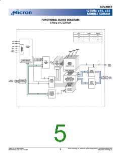
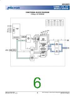
ADVANCE
128Mb: x16, x32
MOBILE SDRAM
FUNCTIONAL DESCRIPTION
Register Definition
In general, the 128Mb SDRAMs (2 Meg x16 x 4 banks
and 1 Meg x 32 x 4 banks) are quad-bank DRAMs that
operate at 3.3V or 2.5V and include a synchronous inter-
face (all signals are registered on the positive edge of the
clock signal, CLK). Each of the x16’s 33,554,432-bit banks
is organized as 4,096 rows by 512 columns by 16 bits.
Each of the x32’s 33,554,432-bit banks is organized as
4,096 rows by 256 columns by 32bits.
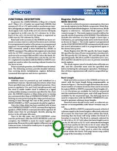
MODE REGISTER
In order to achieve low power consumption, there are
two mode registers in the Mobile component, Mode Reg-
isterandExtendedModeRegister. Forthissection, Mode
Register is referred to. Extended Mode register is dis-
cussedonpage12. Themoderegisterisusedtodefinethe
specific mode of operation of the SDRAM. This definition
includes the selection of a burst length, a burst type, a
CAS latency, an operating mode and a write burst mode,
as shown in Figure 1. The mode register is programmed
via the LOAD MODE REGISTER command and will retain
the stored information until it is programmed again or
the device loses power.
Mode Register bits M0-M2 specify the burst length,
M3 specifies the type of burst (sequential or interleaved),
M4-M6 specify the CAS latency, M7 and M8 specify the
operating mode, M9, M10, and M11 should be set to zero.
M12 and M13 should be set to zero to prevent extended
mode register.
Read and write accesses to the SDRAM are burst ori-
ented; accesses start at a selected location and continue
for a programmed number of locations in a programmed
sequence. Accesses begin with the registration of an AC-
TIVE command, which is then followed by a READ or
WRITEcommand. Theaddressbitsregisteredcoincident
with the ACTIVE command are used to select the bank
and row to be accessed (BA0 and BA1 select the bank, A0-
A11selecttherow). Theaddressbits(x16:A0-A8; x32:A0-
A7; ) registered coincident with the READ or WRITE com-
mand are used to select the starting column location for
the burst access.
The mode register must be loaded when all banks are
idle, and the controller must wait the specified time
before initiating the subsequent operation. Violating ei-
ther of these requirements will result in unspecified op-
eration.
Priortonormaloperation, theSDRAMmustbeinitial-
ized. The following sections provide detailed informa-
tion covering device initialization, register definition,
command descriptions and device operation.
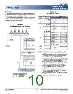
Burst Length
Initialization
Read and write accesses to the SDRAM are burst ori-
ented, with the burst length being programmable, as
shown in Figure 1. The burst length determines the maxi-
mum number of column locations that can be accessed
for a given READ or WRITE command. Burst lengths of 1,
2, 4, or 8 locations are available for both the sequential
and the interleaved burst types, and a full-page burst is
available for the sequential type. The full-page burst is
used in conjunction with the BURST TERMINATE com-
mand to generate arbitrary burst lengths.
SDRAMs must be powered up and initialized in a
predefined manner. Operational procedures other than
those specified may result in undefined operation. Once
power is applied to VDD and VDDQ (simultaneously) and
the clock is stable (stable clock is defined as a signal
cycling within timing constraints specified for the clock
pin), the SDRAM requires a 100µs delay prior to issuing
anycommandotherthanaCOMMANDINHIBITorNOP.
Starting at some point during this 100µs period and con-
tinuing at least through the end of this period, COM-
MAND INHIBIT or NOP commands should be applied.
Once the 100µs delay has been satisfied with at least
one COMMAND INHIBIT or NOP command having been
applied, a PRECHARGE command should be applied. All
banks must then be precharged, thereby placing the
device in the all banks idle state.
Reserved states should not be used, as unknown op-
eration or incompatibility with future versions may re-
sult.
WhenaREADorWRITEcommandisissued, ablockof
columns equal to the burst length is effectively selected.
All accesses for that burst take place within this block,
meaning that the burst will wrap within the block if a
boundary is reached. The block is uniquely selected by
A1-A8 (x16) or A1-A7 (x32) when the burst length is set to
two; by A2-A8 (x16) or A2-A7 (x32) when the burst length
is set to four; and by A3-A8 (x16) or A3-A7 (x32) when the
burst length is set to eight. The remaining (least signifi-
cant) address bit(s) is (are) used to select the starting
location within the block. Full-page bursts wrap within
the page if the boundary is reached.
Once in the idle state, two AUTO REFRESH cycles
must be performed. After the AUTO REFRESH cycles are
complete, the SDRAM is ready for mode register pro-
gramming. Because the mode register will power up in an
unknown state, it should be loaded prior to applying any
operational command.
128Mb: x16, x32 Mobile SDRAM
MobileY95W_3V_F.p65 – Rev. F; Pub. 9/02
Micron Technology, Inc., reserves the right to change products or specifications without notice.
©2002, Micron Technology, Inc.
9

 MICRON [ MICRON TECHNOLOGY ]